
1.1. Introduction to PSpice Simulation
This tutorial is an introduction to Capture CIS and PSPICE simulation. It covers schematic edition and basic SPICE analysis such as BIAS point and DC Sweep using a simple resistor-biased diode circuit as case study.
It uses that circuit to study the static I/V characteristics of a classic PN junction diode.
1. Starting Cadence Allegro Capture CIS
From start menu, launch ![]() Capture CIS 2023 under the Cadence PCB 2023 submenu:
Capture CIS 2023 under the Cadence PCB 2023 submenu:
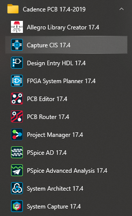
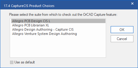
You'll need to specify which license you want to use. Select Allegro PCB Design CIS L, and then OK:
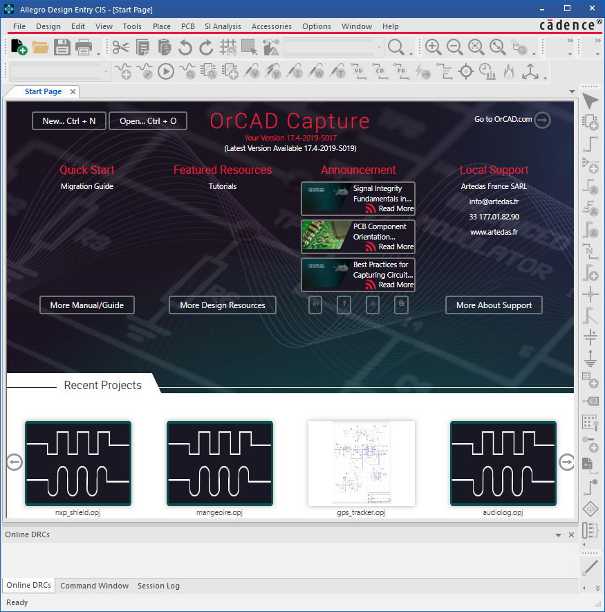
Wait until the application loads. Then maximize the main window:
From the main menu, select File→New→Project or click ![]()
- In the Name field, enter 'tuto_1' as project name.
- In the Location field, choose a folder to store your project files. You may use the
 button to navigate into the file system. One single Cadence project produces a lot of files and subfolders. Take care of your folder structure and keep it clean and organized. On school computers, do not store your files locally (i.e. on C:\). Choose your network P:\ folder instead. For now, you can for instance store this tutorial project in P:\Cadence\tutorials\tuto_1 folder.
 - Make sure you check the Enable PSpice Simulation option since we need this for simulation to work.
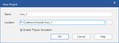
Click OK.
Allegro is now asking for a project template. Keep the default option and click OK again.
The project is initialized and after a short time, you should get a project structure, available in the tuto_1.opj tab corresponding to the tree view below:
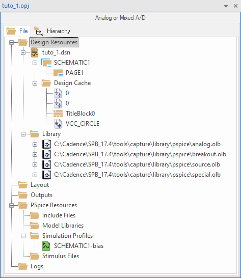
You can explore (expand/collapse) the structure items by clicking in the tree view. If the schematic editor is not open yet, you may just double-click on the PAGE1 item under SCHEMATIC1 folder.
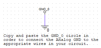
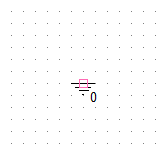
From now on, you're ready to edit the circuit schematic. Default schematic already features the ground symbol 0, which is mandatory for SPICE netlisting (node 0 is always ground). You may perform some cleaning by removing the text field, the GND_0 symbol and the connecting wire:
 |  |
| Before | After |
The ground symbol works as an alias for net 0. Keep it, and duplicate it as much as you need in your schematic (copy/paste, or CTRL-drag).
2. Schematic editing
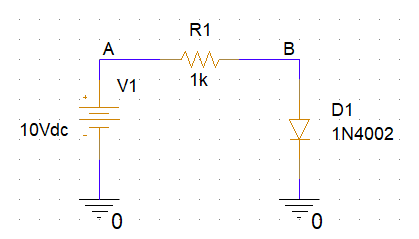
In this tutorial, we will simulate a simple diode biasing circuit. Below is the schematic you have to complete:
There're two ways you can search for and place parts (components) in your schematics:
By using the new dedicated Place → PSpice Part... menu. This tool opens a browser you can use to select parts that are all suitable with PSpice simulation:
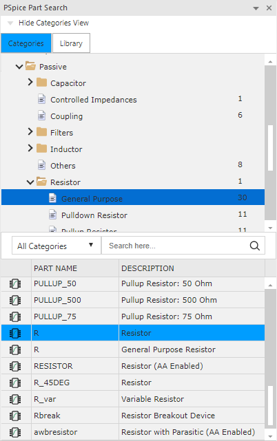
Using this browser, you can pick-up:- Passive → R for the resistor (R1)
- Source → Voltage Sources → DC for the voltage source (V1)Once you have chosen the part you want, just click somewhere on the schematic page to drop it. The keyboard shortcut R can be used if you need to rotate the symbol.
This handy menu only includes generic SPICE parts. It works for passive components (R, C) and sources which are indeed generic. Yet, if you want to simulate a specific component with given manufacturer reference, you need to go for the second way of placing components.
That is the case for the diode (D1). We don't want any generic diode, we want a 1N4002 such as this one :
- By using the standard Place→Part menu entry (or
 ). This action opens the Place Part frame you can use to browse into librarys and parts. Note that here, you can browse all libraries, even those that does not host simulation ready parts.
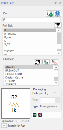
You need to get familiar with commonly used libraries for basic parts such as passive components and voltage/current sources. Be aware that not all parts have an associated Spice model, and therefore can be simulated. For now, you need to know that:
- ANALOG library contains Spice primitive for passive components such as resistors R, capacitors C, inductors L, ...
- SOURCE library contains Spice primitive for voltage and current sources, including constant (VDC, IDC) sources, time-varying sources (VSIN, ISIN, VPULSE, IPULSE...), small-signal sources (VAC, IAC...) and more.
In order to place a new part on the schematic:
1 - Select a library from the list
2 - Double-click the part in the part list. That will stick the new part to the tip of the mouse
3 - Click in the schematic editor page to drop the part at the location you want (you may arrange the part orientation using keyboard shortcuts such as R for rotation or H/V for horizontal/vertical mirrors).
Place the resistor (R from ANALOG) and the voltage source (VDC from SOURCE). Change the voltage value to 10Vdc by double-clicking the actual value on the schematic. Keep 1k$\Omega$ for the resistor value.
For the diode, you need to add a new library that does not appear in the default project. To do that, hit the Add Library button in the Place Part area: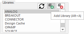
A file system navigator opens to let you choose a new library (.olb) to display. Enter the pspice folder if not already in, and select diode.olb. Note that pspice folder gathers libraries and components that feature associated PSpice simulation models. Libraries and parts outside the pspice folder are most likely not suitable for simulation.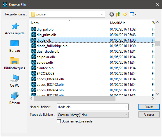
Click Open.
Now, you can place the D1N4002 diode in your schematic page: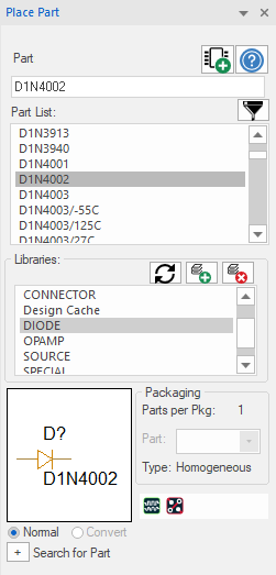
In order to complete the schematic:
Add wires using the button
 (or keyboard shortcut W)
Add net names using the button
 . Provide a name in the Alias field, then click the wire in the schematic page you want to associate with that name.
Be very careful with the ground symbol. You MUST use the symbol that was there at the beginning, or copies of it. If for some reason you deleted that symbol, you may place a new one using the button ![]() , and selecting the '0' part from the list of proposed parts.
, and selecting the '0' part from the list of proposed parts.
When you're done, save the project by right-clicking the tuto_1.dsn item in the project tree view, and then Save.
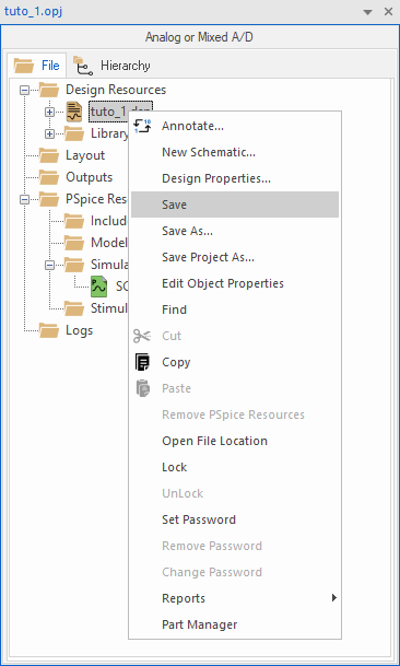
Doing so avoids Cadence asking you to save libraries that doesn't belong to you. This is unfortunately what happens if you use the ![]() button from the main toolbar. The reason for this inconvenience is related to network installation of Cadence products.
button from the main toolbar. The reason for this inconvenience is related to network installation of Cadence products.
3. Simulation Setup (bias point)
PSpice engine allows several analysis to be performed on a circuit. Most common, and the ones you should get comfortable with soon, are:
- BIAS → Static voltages and currents obtained when the circuit is under power supply with no input signal or parameter change
- DC Sweep → Static response to an infinitely slow input or a parameter change
- TRAN → Transient response to time-varying input signal (e.g sine wave, pulse, ...)
- AC → Small signal analysis of the frequency response (e.g. Bode diagrams, small signal linear model assumed)
Each analysis has its own set of parameters. Both the analysis type, and its associated parameters compose something called a simulation profile.
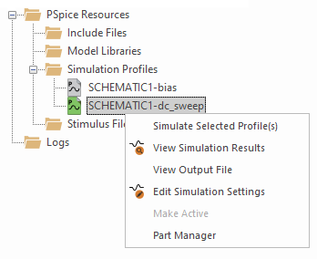
In Allegro, simulation profiles are found under the Simulation Profiles folder of the project tree view, in the PSpice Resources category. If you're lucky, there should already be a bias simulation profile there coming from the default project template. Open the Edit Simulation Settings dialog (![]() )
)
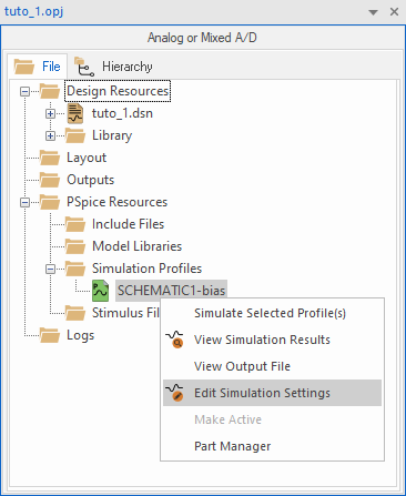
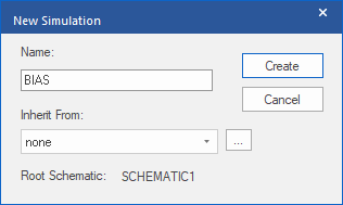
If you're not lucky, you may add a new simulation profile by clicking the![]() button. Name the profile (e.g. BIAS) and create it.
button. Name the profile (e.g. BIAS) and create it.
In the Simulation Settings dialog review the simulation settings carefully:
- Analysis type should be Bias Point
- Check the .OP option in the Output File Options section
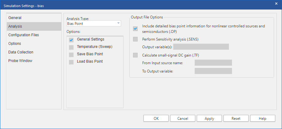
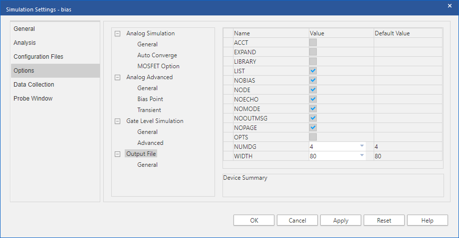
In the Options category, make sure you have the following checked:
Once you're done reviewing the simulation settings, click Apply, and then OK.
4. Running the simulation
Click the ![]() button from the main toolbar and open your eyes!
button from the main toolbar and open your eyes!
Simulation is a two-step process:
- First the schematic is converted into a SPICE netlist file
- Second, the simulation engine performs calculation based on the netlist file and simulation settings
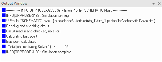
The first step execution (netlist) is reported into the log region of the main window:
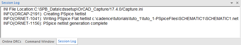
Netlist creation may fail for several reasons. A common case of failure is the use of parts (component) in your schematic that are not associated to any Spice simulation model (i.e. a set of mathematical equations describing the component behavior). You need to take a look on this report every time you launch a simulation.
The second step causes a new window ![]() Allegro PSpice Simulator to open.
Allegro PSpice Simulator to open.
In the bottom ribbon, you'll find the simulation execution report. Get used to read this report every time you run a simulation. When simulation fails, you may find clues here of what happened. Trough, information here is not always easy to understand for beginners.
5. Results review
Do not close the Allegro PSpice Simulator window, but go back to the schematic editor page. Toggle both voltage ![]() and current
and current ![]() annotation buttons. You should get new labels indicating static voltages on every circuit nodes, and currents entering each part. You can mouse-drag those labels for better visibility:
annotation buttons. You should get new labels indicating static voltages on every circuit nodes, and currents entering each part. You can mouse-drag those labels for better visibility:
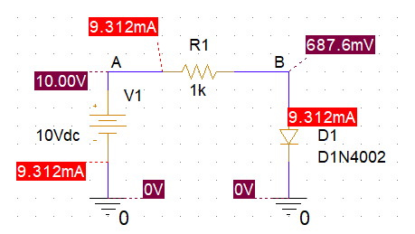
On such a simple case, you can easily verify that Spice is providing credible results (do not misunderstand me... Spice works well, of course, but your input files may not...). Here, the voltage across the diode is $V_{D1}=0.69V$, which is an expected result. The current in the unique branch is limited by the resistor to $(10-0.69)/1000 = 9.31mA$.
Everything looks fine!
Now, bring the Allegro PSpice Simulator window under focus. From the main menu, open View→Output File (![]() ).
).
Having a look to this file is very important. For now on, let us concentrate on few sections:
- The SPICE formatted circuit netlist. Highly useful to find out schematic errors. This netlist simply lists schematic parts with nodes (wires) names connected to part terminals, and parameters such as components values. It is therefore nothing more than a text representation of the exact same schematic you edited graphically.
//**** INCLUDING SCHEMATIC1.net ****
//* source TUTO_1
R_R1         A B  1k TC=0,0
V_V1         A 0 10Vdc
D_D1 B 0 D1N4002 - Model parameter set for components. Below is the model parameter set associated to the 1N4002 diode. Those parameters are characterized by the component manufacturer (foundry) and applied to a generic physical model (equation set) representing any diode behavior. What makes a diode different from another is this parameter set. Here, you may notice known parameters such as IS (inverse saturated current) or N (lambda) the tuning coefficient of the Shockley law.
//****     Diode MODEL PARAMETERS
//***********************************
               D1N4002
          IS   14.110000E-09
           N    1.984
         ISR  100.000000E-12
         IKF   94.81
          BV  100.1
         IBV   10
          RS     .03389
          TT    4.761000E-06
         CJO   51.170000E-12
          VJ     .3905
           M     .2762
Chance is that several parameters are beyond your knowledge. Keep in mind that Shockley law is a very rough approximation of the diode behavior. SPICE model implements way more sophisticated equation set to simulate diode physics, including thermal dependency, slope saturation at strong current, and parasitic capacitance to mention few.
Anyway, one should understand right now that model parameter set is related to the component design and fabrication, and is valid for all part of same reference (1N4002 here). It is therefore completely independent to the role the component plays in the circuit under analysis.
- Bias point calculation: Based on model parameters, and the circuit topology, the simulator engines then calculate voltage at each node, and currents delivered by power generators.
//****     SMALL SIGNAL BIAS SOLUTION       TEMPERATURE =   27.000 DEG C
//******************************************************************************
 NODE   VOLTAGE     NODE   VOLTAGE     NODE   VOLTAGE     NODE   VOLTAGE
(    A)   10.0000  (    B)     .6876
    VOLTAGE SOURCE CURRENTS
    NAME         CURRENT
    V_V1        -9.312E-03
    TOTAL POWER DISSIPATION   9.31E-02  WATTS
Don't get confused with the header "SMALL SIGNAL BIAS SOLUTION". This is not the result of a small signal analysis. This is the static bias point calculation (static voltages and currents). Nevertheless, remember that small-signal parameters (local derivatives) for non-linear components (the diode here) depends on biasing conditions (i.e. the point where the local derivatives are calculated). Therefore, the bias point is the key to compute small-signal parameters for non-linear components.
- Small-signal parameters for non-linear components. Those depends on the bias point calculation, and therefore in the circuit topology. Contrary to the model parameters set, results may differ from one diode to another of same reference if you have many in a given circuit. One can see here that in our case, the diode equivalent small signal resistance around the biasing point is 5.5$\Omega$.
//****     OPERATING POINT INFORMATION      TEMPERATURE =   27.000 DEG C
//******************************************************************************
//**** DIODES
NAME         D_D1
MODEL        D1N4002
ID           9.31E-03
VD           6.88E-01
REQ          5.51E+00
CAP          8.64E-07
6. Static transfer characteristic (DC sweep)
A static characteristic corresponds to the evolution of the biasing point with respect to a varying input parameter. This varying input parameter can be anything you want to study: a voltage, a current, a component value (i.e. the resistor value), a model parameter... No dynamic effects are taken into account in such analysis. In other words, you may consider that the input parameters varies with an infinitely slow speed. For each input value, the obtained result would therefore be the one obtained after the circuit reaches a perfeclty steady state. That's what explains the word 'static' for this transfer function. The collection of input values is specified with a range (from...to) and a step (or a number of points). That's why it's called a sweep.
For now, you may close the Allegro PSpice Simulator window and go back to the project resource tree view.
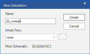
Let us define a new simulation profile ![]() (or from the main menu PSpice→New Simulation Profile). Give a name (e.g. 'dc_sweep') to the profile and then click Create:
(or from the main menu PSpice→New Simulation Profile). Give a name (e.g. 'dc_sweep') to the profile and then click Create:
Review the simulation settings:
- Analysis type must be DC Sweep
- The varying parameter (Sweep Variable) is the voltage source V1
- The Sweep Type is a linear sweep of V1 voltage, from 0V to 2V with one point every 1mV (for a total of 2000 bias points to be calculated)
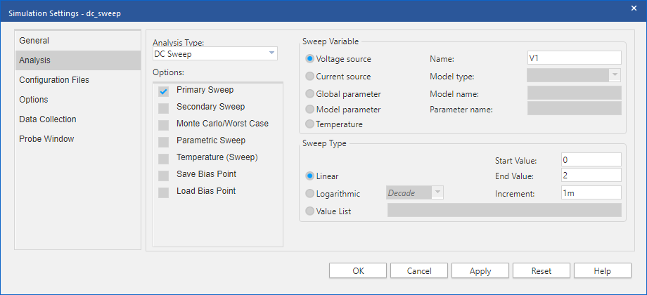
When you're done, click Apply, and then OK. Make sure that the new simulation profile has been added to the resource tree view, and is now active (green icon). If not, you can right-click on the profile item and select the Make Active menu entry.
You may also check that the new simulation profile is selected in the drop-down list of the main toolbar:
![]()
Now run ![]() the simulation and check both log reports, just like we did before. If everything goes well, the Allegro PSpice Simulator window comes back with an empty graph. You may notice that x-axis is already labeled and scaled according to your input variable (V1, from 0V to 2V).
the simulation and check both log reports, just like we did before. If everything goes well, the Allegro PSpice Simulator window comes back with an empty graph. You may notice that x-axis is already labeled and scaled according to your input variable (V1, from 0V to 2V).
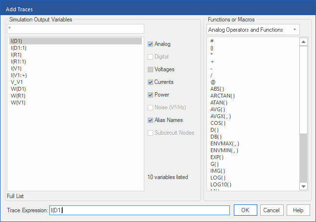
From the main menu select Trace→Add Trace or click ![]() .
.
Say we want to analyze the current through the diode as a function of the input voltage. Select I(D1) in the Simulation Output Variables list and make sure your selection appear in the Trace Expression field at the bottom of the dialog window. Then click OK.
The result is displayed as a curve:
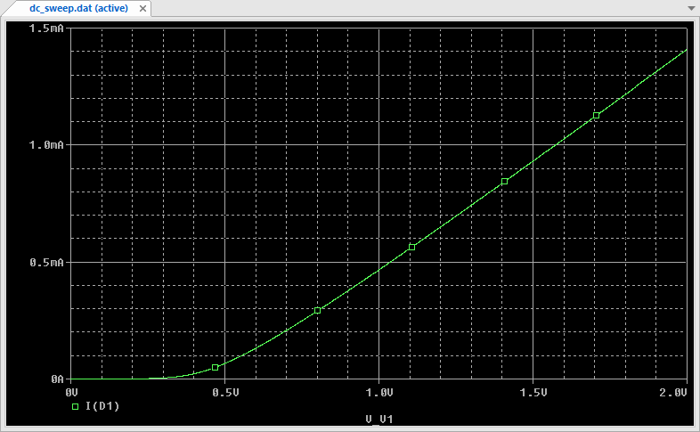
Does this characteristics represent $I_{D1}=f(V_{D1})$? Of course not, since x-axis is V1 voltage and not the voltage across the diode $V_{D1}$. A trick would be to repeat the simulation with R1 value set to 0$\Omega$. We'll see another method.
Click once into the plot, and then from the main menu select Plot→Axis Settings.
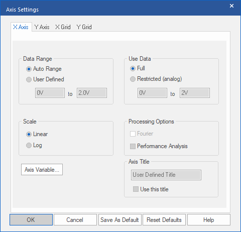
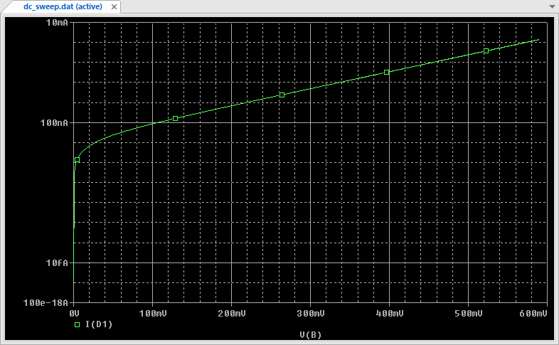
In the dialog box, click the Axis Variable button and select V(B) from the list of possible variables. $V_B$ is actually same as $V_{D1}$ since the diode cathode is grounded. Click OK and then OK to close both dialogs. The updated plot now corresponds to the expected $I_{D1}=f(V_{D1})$ transfer characteristic. Use this curve to evaluate the knee voltage for this diode.
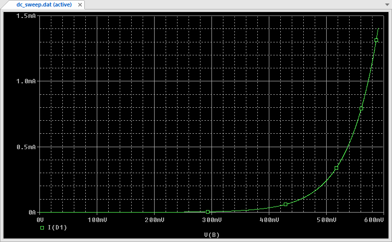
Click the ![]() button to turn y-axis into log scale. Do you see any knee now?
button to turn y-axis into log scale. Do you see any knee now?
From this point, do not hesitate to explore the user interface and find utilities by yourself. Cursors ![]() are helpful for measurements. You can drag both cursors using left and right mouse buttons.
are helpful for measurements. You can drag both cursors using left and right mouse buttons.
7. Final tip
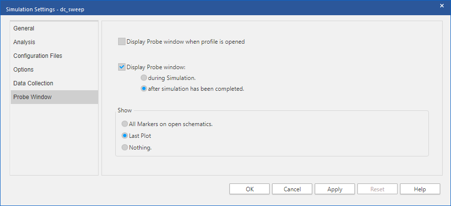
Every time you'll run the same simulation (after minor changes in the schematic), you'll have to repeat the trace selection procedure. That's somehow painful, especially during iterative design process. To keep traces from one simulation to the next one, you need to go back to the simulation profile settings and check the Last Plot option in the Show section of the Probe Window category.
Try it, you'll love it!
When you're done, you can close everything!
- Log in to post comments