
2.6. Fabrication files
Time has come to fabricate your PCB? You need to provide the fabrication facility, either professional or DIY (CNC) with:
A set of files that defines the board outline, tracks, pads, shapes... These are in Gerber format
A file that defines holes drilling in NC/Excellon format
1. Preliminary checking
Review your board carefully. At this step, you're supposed to be ready for fabrication. It means that you'll engage expenses (time and materials) so you better be sure of what you've done.
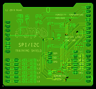
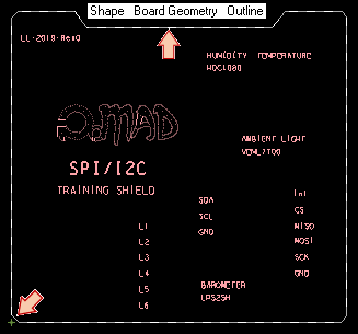
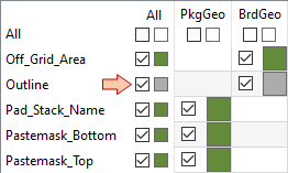
Tuning layer visibility in the color editor ![]() , check that you have a board outline definition, and that design origin is set close to the board. If the board outline is missing, you need to add one using shape tools (
, check that you have a board outline definition, and that design origin is set close to the board. If the board outline is missing, you need to add one using shape tools (![]() , ...).
, ...).
 |  |
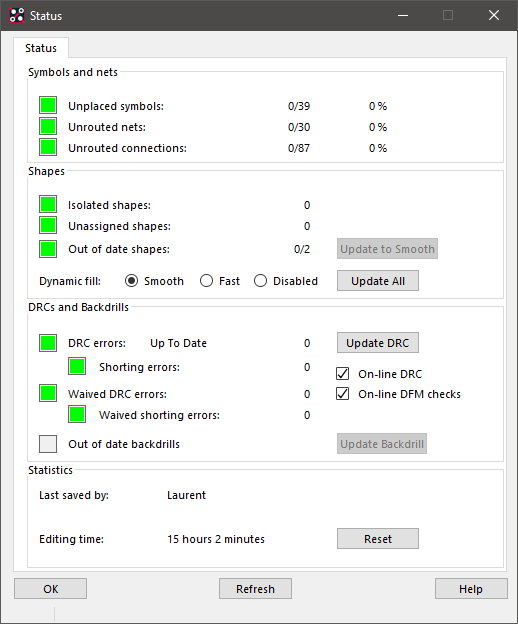
Make sure everything is placed and routed by checking Display→Status. You may have some isolated shapes, and maybe some DRC errors you understand and leave. That's OK. Nets and symbols must be 100% placed and routed. Shapes must be up-to-date.
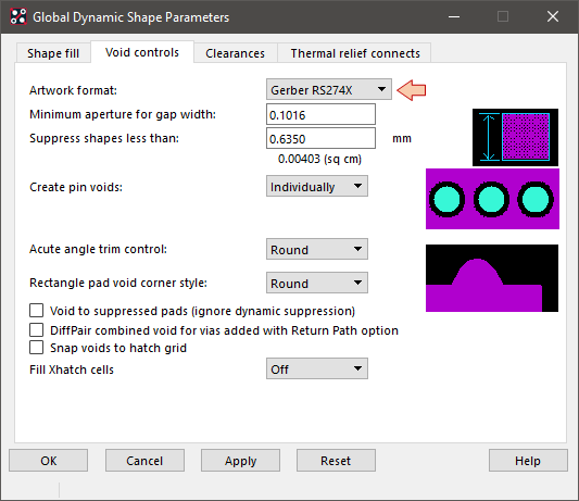
You may update shapes using Shapes→Global Dynamic Params... from the main menu:
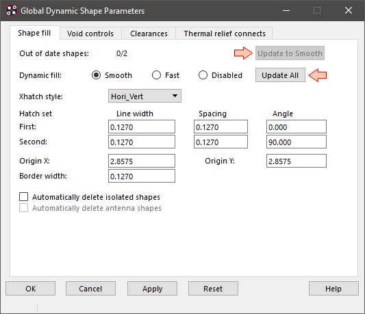
And then make sure that dynamic shapes are in the Gerber RS274x format:
2. Creating GERBER files
Open Manufacture→Artwork.
In the Film Control tab, you need to populate the Available films list with fabrication layers. The list depends on the fabrication facility you target. For DIY PCBs, you only need outline and copper layers. For professional fab, you need to provide more layers including soldermasks, silkscreens, and perhaps pastemasks if you order stencils.
Note that, in the lists below, each folder produces a separate fabrication file (named after the folder name). Each file embeds all the included layers within a folder.
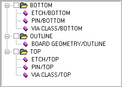 | 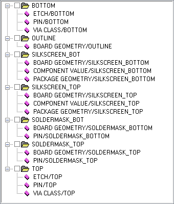 |
| Typical film list for DIY CNC routing. Only outline and copper (etch) films are required. | Typical film list for professional fab. Beside outline and etch films, soldermask is absolutely mandatory. Optionally you may also provide silkscreens and pastemasks (stencil). |
 |  |
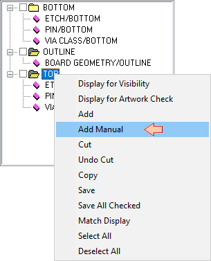
You can build your own list by right-clicking on film folders and layers and then use Add, Add_manual and Cut menu entries.
For example, starting with the default list. Select the TOP film, and then do right-click→Add Manual:
Provide a name for the new film:
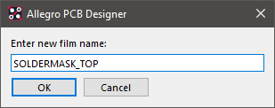
Then select the subclasses you want to add to this film. In this case:
BOARD GEOMETRY / SOLDERMASK_TOP
PIN / SOLDERMASK_TOP
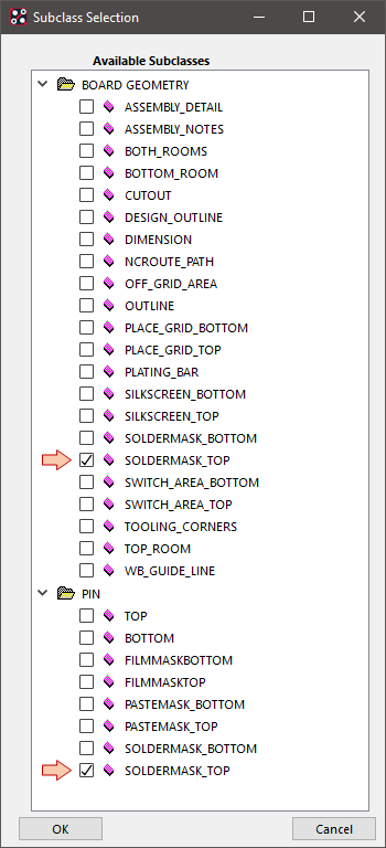
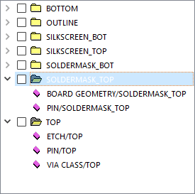
Click OK. You're done adding a new Gerber film:
You may also Add/Cut layers to an existing film folder by right-clicking on any layer item belonging to that film.
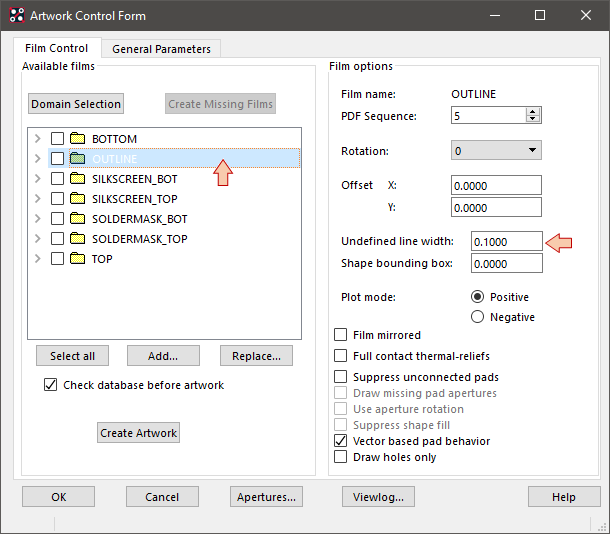
When you're done preparing the film list, select the OUTLINE film and set the Undefined line width to something small but not null. Actually, the board outline is made of a zero-thickness contour line. If we forget this, no outline film is produced by the artwork generator engine.
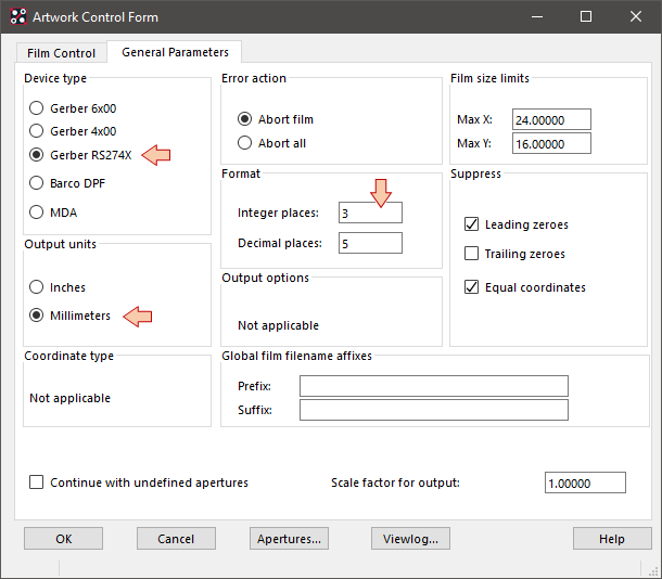
Now open the General Parameters tab and review parameters. You may adjust coordinates format (Integer places / Decimal places) according to the size of your board. Below settings will work in most cases.
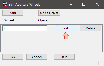
Then click the Apertures... button. In the Edit Aperture Wheels dialog click the Edit... button of Wheel #1:
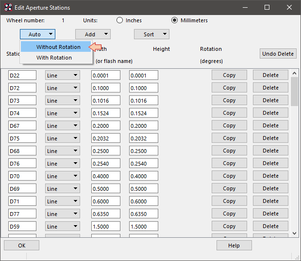
Then select Auto-> → Without Rotation. This will create the aperture list. Click OK when its done.
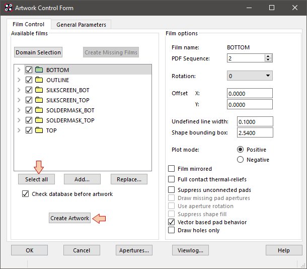
Almost done... Back to the Film Control tab, click Select all so that all the films are selected, and then Create Artwork.
You may get a warning dialog window regarding the choice of the outline layer. You can ignore that warning and continue artwork generation.
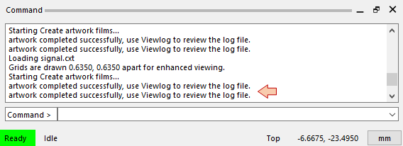
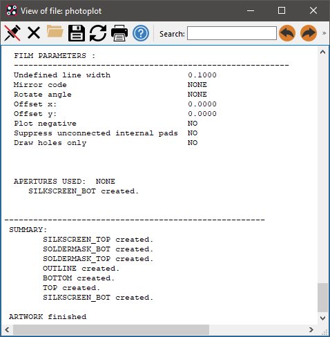
Carefully monitor the Command log in the main window to make sure the artwork completes successfully:
Then click the Viewlog... button in the Artwork Control Form. Scroll down to the end of the log and make sure all films have been created:
You may close the Artwork Control Form by clicking OK.
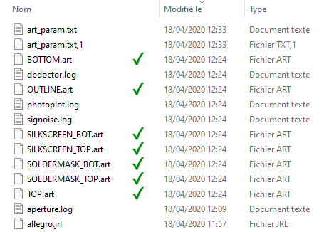
Navigate into your design folder and check that the artwork files (.art) are there for all films:
3. Creating DRILL file
Open Manufacture→NC→NC Drill...
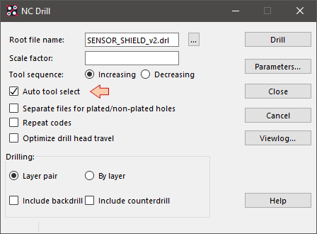
Review settings, then click the Parameters... button.
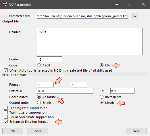
Again, review settings to match those shown above. Then close the NC Parameters dialog.
Back to the NC Drill dialog, click the Drill... button.
Again, carefully monitor the command log in the main window to make sure the NC Drill completes successfully:
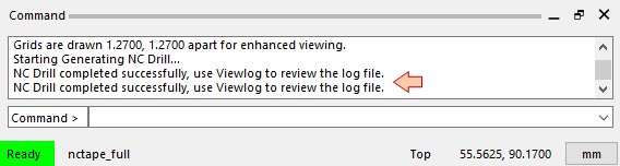
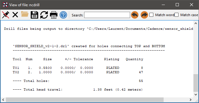
Then click the Viewlog... button in the NC Drill dialog. Scroll down to the end of the log and make sure the drill file has been created:
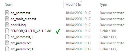
And again, navigate into your design folder and check that the drill file (.drl) is there:
4. Final verifications
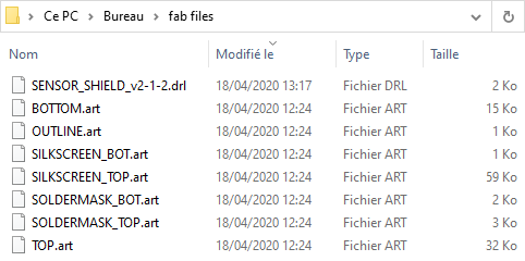
You can now collect (copy) all fabrication files into a separate folder in order to make an archive (.tar, .zip, .7z...) you can send to the fab:
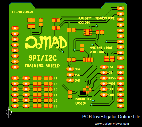
You'll find several online Gerber viewer on the internet. Many PCB manufacturers now offer such service, but all doesn't support Cadence files very well. That's a good idea verifying your Gerber and Drill files using such tools.
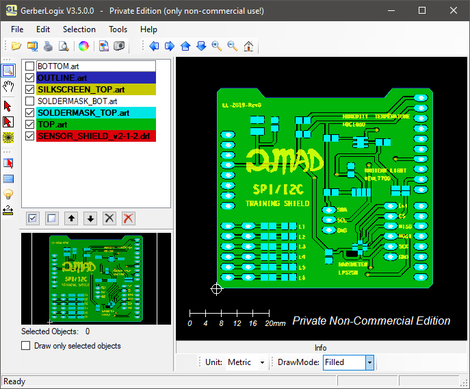
Personally, I've been using a windows application for years that is freely available from Easylogix. It's called GerberLogix and it comes as a portable single executable file you may also get from here if the previous link is broken. It's very convenient for viewing Gerbers and Drills. It supports Cadence outputs, and you can even perform distance measurements:
- Log in to post comments