
2.5. Logos and mechanical parts

1. Preparing the logo
You can import vectored pictures in Cadence using its DXF import capability. For this, you'll need first to convert the picture into the Autocad DXF format. Almost any mechanical CAD software can do that. I'm personally using a DXF export plugin with Sketchup. Yet, in this tutorial, I'll illustrate an example using Inkscape free drawing software as a starting point.
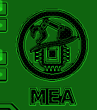
So let assume that you have a vectored picture available in Inkscape:
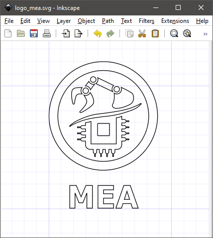
You need to pay attention to the size of the picture here because Cadence can by no means rescale the drawing after import. The size in Inkscape is the size you'll get on the PCB at the end. Turn units in mm and rescale the drawing as you need. In the above example, the grid pitch is 1mm, so that logo is 12mm in height, and 9mm in width.
When you're OK with the size, save the drawing as a DXF file:
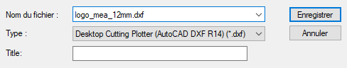
You may need to set export options. Use polylines instead of splines:
2. Importing the logo into a Mechanical symbol
Next step, open Cadence ![]() PCB designer and start a new drawing.
PCB designer and start a new drawing.
File→New. Set the New Drawing options as follows:
Drawing Type: Mechanical symbol. Mechanical symbols are basically the same thing as Package symbols except that there is no link with the electrical netlist from Capture. You can therefore freely place mechanical symbols on your PCB with no electrical constraints. A common example of mechanical symbol you may use are mounting holes.
Drawing Name: Choose a path and a name for your part. In this example, the part name will be 'logo_MEA_12mm.dra'. Choose or create a directory to store your mechanical symbols. It can be the same as for package symbols, or a different one. It's up to you. Here, I'm creating the new part into tutorials\pcblib\symbols\ directory.
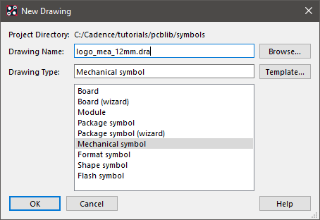
Click OK.
As usual, start by tuning units and grid parameters. Set units to mm and grid pitch to 2.54mm. Go to Setup → Design Parameters ![]() and make sure settings are as follows:
and make sure settings are as follows:
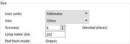
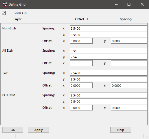
Click Apply and OK.
From the main menu, now select File→Import→DXF...
Using the ![]() button, browse and select the DXF file you saved earlier.
button, browse and select the DXF file you saved earlier.
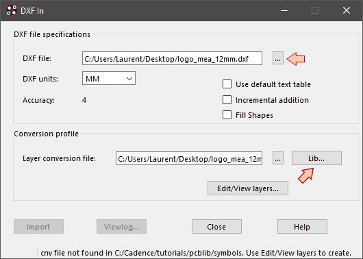
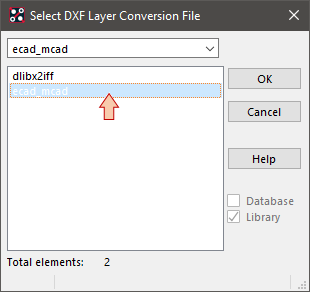
In the Conversion profile area, click the Lib... button. Select ecad_mcad conversion file and click OK.
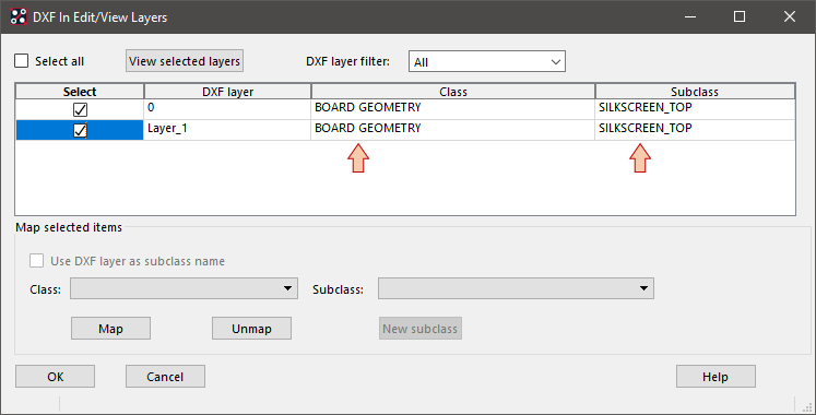
In the DXF In dialog, now click the Edit/View layers... button. Select all the available DXF layers (this depends on the CAD tool you've used to export the DXF file) and choose a target Class/Subclass for the conversion. I suggest using the top silkscreen layer for a start. That's the commonly used layer for printing logos on PCB, and you can change this later if you need. When you're done, click OK.
Back to the DXF In dialog, now click Import. You will see a dialog with import progress bar and then a report of success:
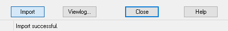
Click Close. You're done importing the DXF drawing.
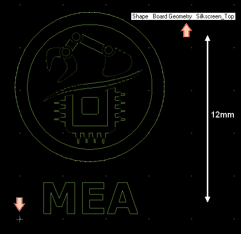
Try and find the imported logo in the working area... It can be everywhere because it depends on the actual origin (0,0) in your drawing software, and the actual origin point within Allegro. Use zoom in/out to search where it is located.
Then perform the following verifications and adjustments:
Place design origin close to the logo (Setup→Change Drawing Origin). This is important because origin is the mouse handle when placing the logo later on.
Hover the mouse over the drawing lines and check that class/subclass used for import is Silkscreen_Top as expected.
Make sure the dimensions are OK based on the grid or use the ruler
 .
.
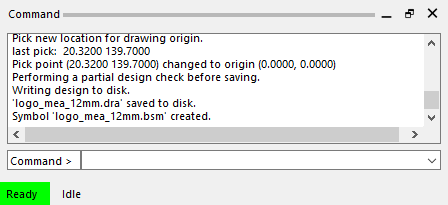
Save the design ![]() . Make sure that the mechanical symbol is created:
. Make sure that the mechanical symbol is created:
3. Placing the logo onto the board design
Open the board file you want to place the logo on. Tune colors and visibility to clean the display and show only the top (or bottom) copper layer:
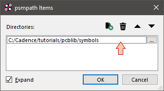
Open Setup→User Preferences... In the Paths→Library category, add the path to your logo folder to the psmpath Items.
Click OK and exit the User Preferences Editor.
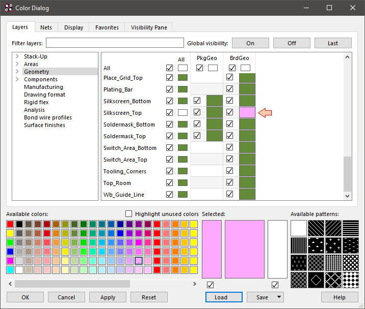
Now, open the Color Editor ![]() and let us change the top Silkscreen layer (Board Geometry) to something easy to recognize (e.g. pink). That's the layer we've used before to create the logo. Click Apply when done.
and let us change the top Silkscreen layer (Board Geometry) to something easy to recognize (e.g. pink). That's the layer we've used before to create the logo. Click Apply when done.
Then, from the main menu, select Place→Manually ![]() .
.
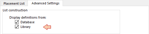
In the Advanced Settings tab, check the Library option in the List construction box:
In the Placement List tab, select Mechanical symbols. You should see the list of available mechanical symbols that probably differs from the figure below. At least, you should see the 'LOGO_MEA_12MM' symbol.
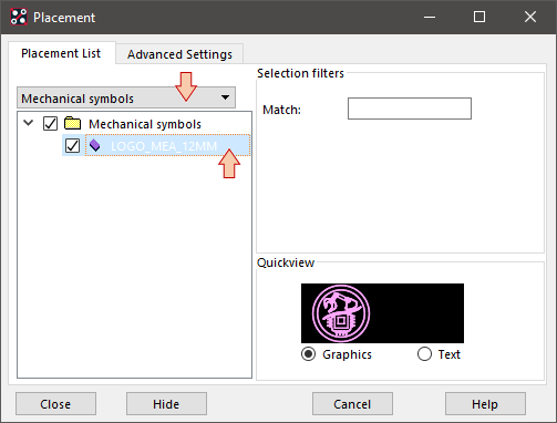
Select the logo. From there, you can place it on the board area, just like any component you've placed before. Place the logo apart from the board for now, since we have some edits to perform prior its final placement:
From there, you face several options to set the appearance of the logo on the board:
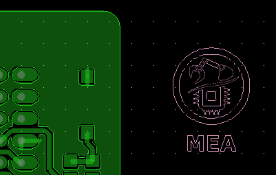
If you go to professional PCB manufacturing, you'll have the silkscreen layer available. If you go through DIY, the only available layer is the copper layer. In this case you'll have to change the logo layer (class/subclass) from Silkscreen to Etch.
You may want plain logo, or outlined logo. Up to your taste
 |  |  |
| Plain logo on silkscreen | Outlined logo on silkscreen | Copper engraved logo |
At this step, your logo is made of shapes that are only defined by lines (not areas) with null thickness. Placing the logo as it is now would do nothing. You can:
Change the logo into plain shapes using Shape→Compose Shape (review options, and then select the whole logo using a rectangle box).
Change the logo into lines of adjustable width using Shape→Decompose Shape (review options, and then select the whole logo using a rectangle box), then you may change line width using contextual menu.
Using the Options panel while running these tools, you can change the class/subclass (i.e. the layer) of the logo if you want.
Once the logo has been prepared, you can move it ![]() to the location you like on the board. Here are examples of what you can achieve playing with options and shape tools:
to the location you like on the board. Here are examples of what you can achieve playing with options and shape tools:
 |  |  |
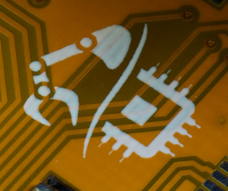
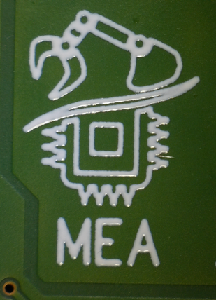
| Plain Shape (Compose) on Silkscreen layer. Most common for professional fabrication | Plain Shape (Compose) on Etch layer. OK for DIY | Plain Shape (Compose) on etch layer with subsequent XORing of the ground plane. Nice for DIY |
 |  | |
| Outlined (Decompose) on Silkscreen layer and line width changed to 0.2mm | Outlined (Decompose) on Etch layer and line width changed to 0.2mm. Placed into a ground plane rectangular void. Not recommended for DIY | |
If you always process your logos the same way, you may consider doing the edit at symbol level so that you can directly place it in the board.

- Log in to post comments