
2.7. 3D rendering
By these days, 3D rendering is a feature you can find in almost all PCB CAD suite on the market. Beside allowing nice pictures to be created, it offers export of board 3D models toward mechanical CAD software for further integration. That's highly useful.
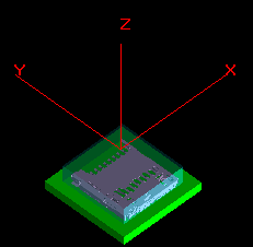
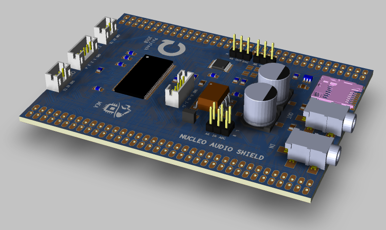
Cadence Allegro has such a 3D rendering and export engine. Let's take the audio shield from the clonewheel project as an example. Starting point is a finished board design. You can use any of yours to practice along this tutorial.
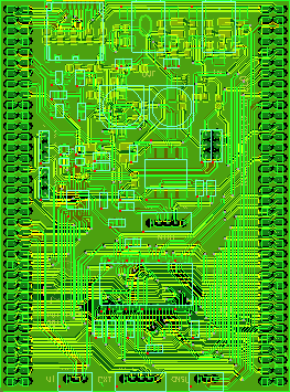 | 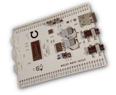 |
| Audio shield board design | Picture of the (real) assembled board |
1. Allegro 3D Canvas tool
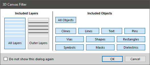
Open an existing PCB design, and click the ![]() button right away.
button right away.
The 3D Canvas Filter dialog opens. Make sure that everything is on display and click OK.
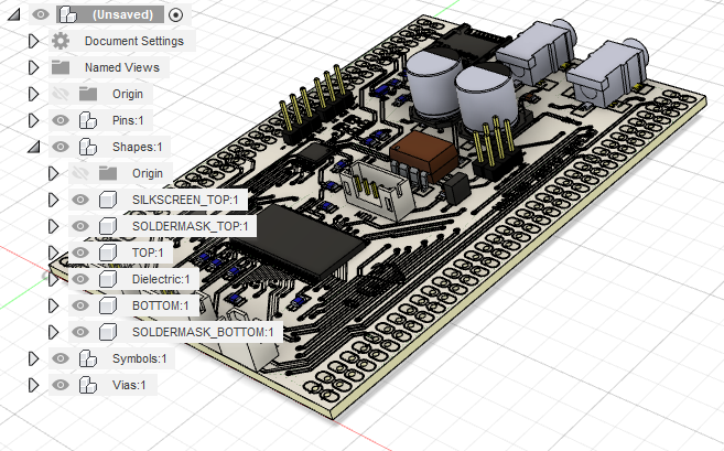
This generates a default 3D rendering of the board and opens the Allegro 3D Canvas dialog:
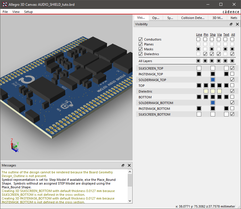
Choose your preferred color scheme using the Setup → Preferences dialog.
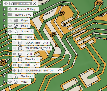
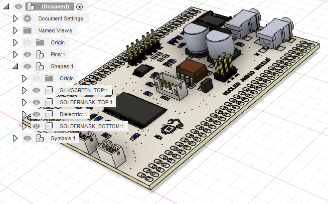
You can use the Visibility panel, or the Symbol panel to toggle layers/components you want to see or not. For example, removing all except Dielectric, TOP and BOTTOM layers, you get something pretty close in appearance to the bare PCB from a CNC DIY fabrication process:
You can click the mouse middle-button (wheel) to move/pan the board. While pressing the shift key, the same operation rotates the 3D view. Very nice!
As you can see, so far, components are roughly represented by simple black boxes based on the package outline found in the symbol design, with fixed height. This is what Cadence calls the Boundary Shapes.
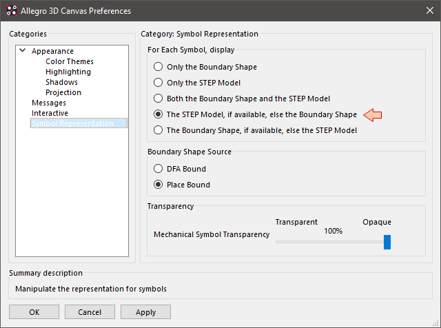
You can tune the preferences so that theses Boundary Shapes are displayed when no valid 3D model is found:
And that's where the fun begins...
To go further, you'll need to collect 3D models of all parts on the board. Hopefully, you'll find most (if not all) 3D models already available somewhere on the Internet.
Here are some 3D model repositories you may look at :
GrabCAD (https://grabcad.com)
3D Content Central (https://www.3dcontentcentral.fr)
Radiospares, Digikey and other distributors provides 3D models (or links) for a lot of electromechanical (i.e. sockets, connectors, ...) parts
Part manufacturer websites
Cadence requires 3D models to be provided in the STEP format.
Typically STEP can be used to exchange data between CAD, computer-aided manufacturing, computer-aided engineering, product data management/enterprise data modeling and other CAx systems. STEP addresses product data from mechanical and electrical design, geometric dimensioning and tolerancing, analysis and manufacturing, as well as additional information specific to various industries such as automotive, aerospace, building construction, ship, oil and gas, process plants and others. STEP is developed and maintained by the ISO technical committee TC 184, Automation systems and integration, sub-committee SC 4, Industrial data. Like other ISO and IEC standards STEP is copyright by ISO and is not freely available. However, the 10303 EXPRESS schemas are freely available, as are the recommended practices for implementers. https://en.wikipedia.org/wiki/ISO_10303
2. Assigning a STEP model for each part
2.1. Gathering STEP 3D models
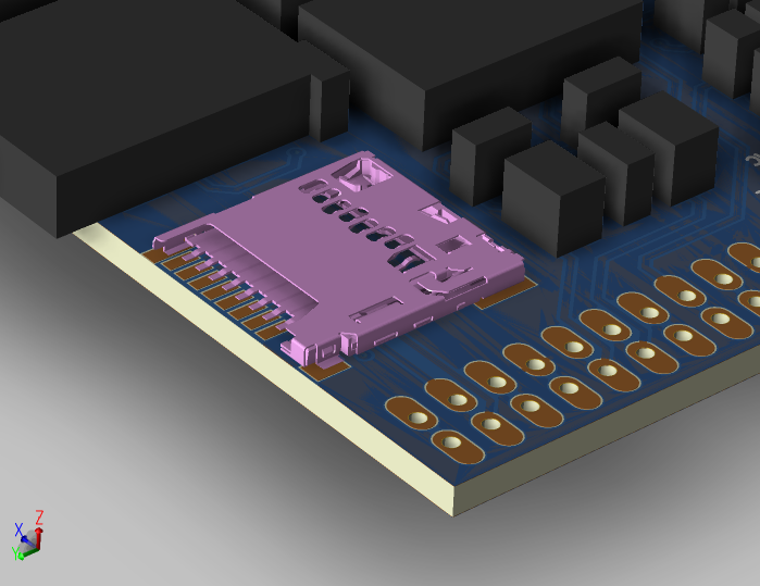
Let us start with the SD Card socket. This one is a MOLEX part from their 503398 series. Your best option is always to find a 3D model directly from the manufacturer website. We're lucky this time, because MOLEX does provide 3D models for this socket.
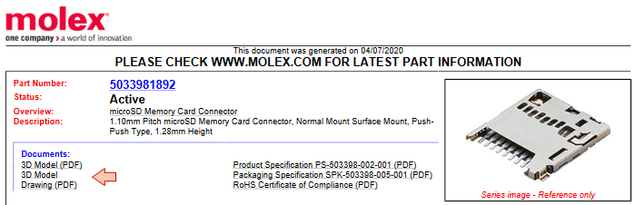
Even more luckily, MOLEX provides models in CREO, IGES and STEP formats. After downloading the STEP model, we can open it in our preferred 3D CAD software to see what it is like. I'm using Autodesk® Fusion 360® here to open the STEP file:
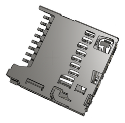
It seems alright, so let's take this into Cadence.
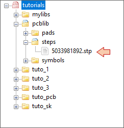
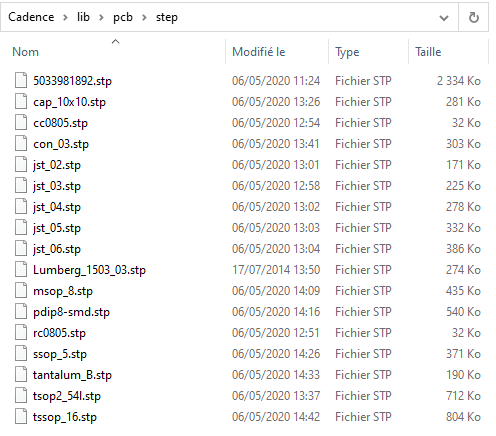
First, you'll need a dedicated folder to store your 3D STEP files, just like for symbols. I'm using a tutorials\pcblib\step\ folder in my own file organization. You can have it anywhere you like. Create such folder and move the STEP file (.stp) into it:
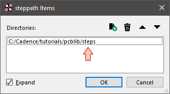
Second, you need to setup a path to that folder. Within Allegro, go to Setup→User Preferences..., then in the Path→Library category and edit the steppath item in order to include the path to your step\ folder:
Apply and exit the setup dialogs.
2.2. Assigning each part symbol a STEP model
The next step consist in mapping STEP models to PCB symbols. This process involves two things:
Choosing a STEP file for each symbol in your PCB design
Performing a manual 3D alignment of the physical model with the footprint (translations/rotations) so that the model perfectly lands on the footprint.
Since SPB 17.4 version, you have 2 options for performing the symbol/3D mapping:
The legacy tool you can launch using the menu Setup→Step Package Mapping...
From within the 3D canvas itself
The second approach, using the 3D canvas, is more user friendly. Yet, let-us give a try of both.
The legacy method:
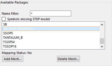
Open the Setup→Step Package Mapping... interface. This dialog is designed to assign STEP models to Allegro symbols. This mapping involves:
To choose a STEP file for each part (i.e. each symbol) on the board
Because there is obviously no consistency in the origin, offset and rotation between the STEP model and the foorprint, you need to manually fit the 3D model onto the corresponding symbol footprint (only once per symbol, hopefully).
Make sure that the interface is in the Package mode. Most of the time, you want to associate a STEP model with a package, not a device. Basically, all '0805' resistors can use the same STEP model and you don't want to repeat association for each individual resistor.
You have two lists:
The symbol list (those in your PCB design)
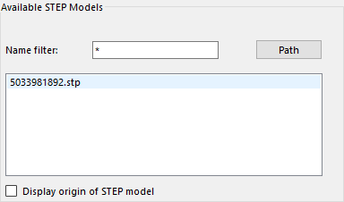
The STEP model list (those in your /step folder)
In each list, pickup the symbol and the STEP model you want to associate:
 |  |
Then, look at the actual alignment between the two descriptions. You may enable the Overlay option to achieve the same view:
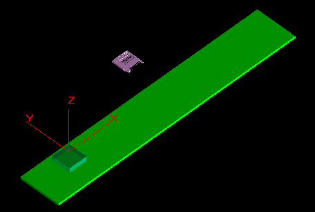
Now play with the control panel to achieve the best alignment you can between the footprint and the STEP model (using arrows, views, rotations):
It can be quite tedious to refine the alignment, so use all the available views (front, left, top, ...) to make sure it is good:
 |  |
When you're happy, click Save and then Close the dialog.
Quit the 3D Canvas if it is still opened, then hit the ![]() button again. The socket is there, and well placed!
button again. The socket is there, and well placed!
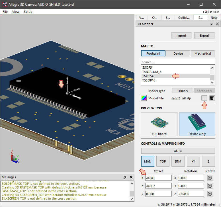
Using the 3D Canvas:
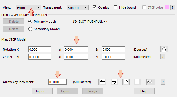
You can directly map and align 3D models from within the 3D Canvas using the 3D Mapper tab. It is quite simple and provides better visualization for aligning 3D models with the footprint:
Select the footprint you want to map a 3D model with
Browse for the corresponding STEP file
Choose the preview mode (Device Only helps focusing on the current part)
Use controls together with different camera views (Top, Left, Front, ...) to perform the model positioning. Manual mode allows for direct dragging of the 3D model in the 3D rendering view. Smart!
Well, that's pretty much it... You'll need to repeat above steps for ALL the symbols you have on your board... Good luck, it takes some time to find good-looking STEP models and to refine footprint alignment. For this board, I found most STEP models on 3D Content Central, except for jack connectors that were available from the manufacturer (Lumberg©).
Here is the complete list of STEP models that were necessary:
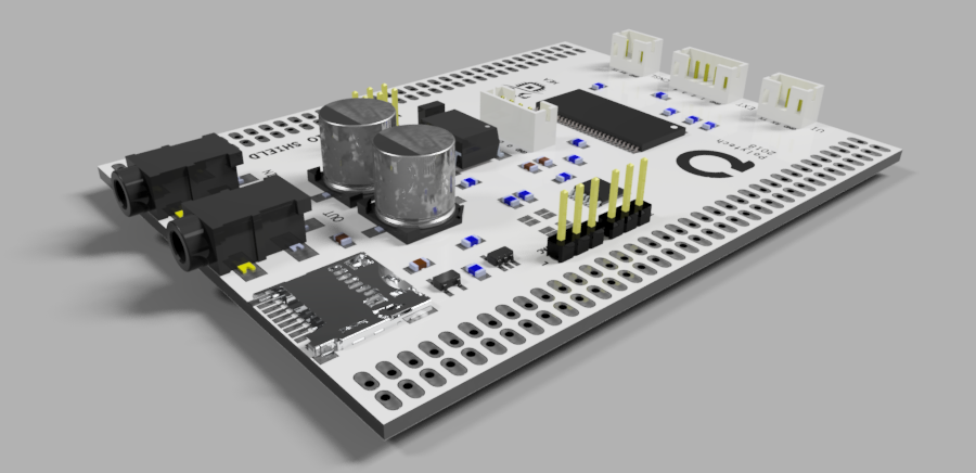
And the final result in result in Allegro:
3. Finishing and exporting board model
From that point, you may export the board as a STEP mechanical model. You can either use the File→Export command available from the 3D Canvas dialog, or go to File → Export → STEP... from the main menu. The latter has more options to select objects/layers you may discard from the export process.
Actually, the full STEP export produces a huge file with a lot of details including internal tracks, pins and vias modeling to mention few. In my example, the board STEP file is 67MB heavy.
The picture below shows the exported model when opened in Autodesk® Fusion 360®. Note the fully hierarchical structure of the model including every details:
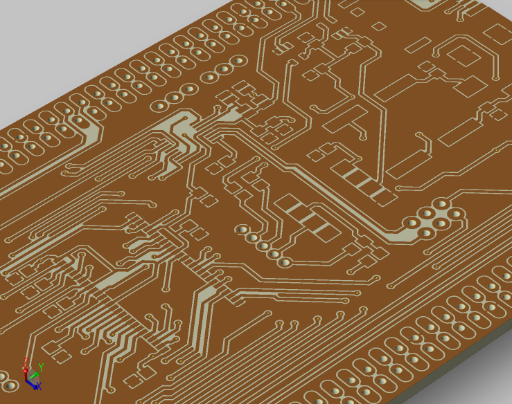
For example, layers TOP, BOTTOM, Pins and Vias provides full 3D modeling of copper tracks and thru holes:
For mechanical integration you may not need such details. Here is the same board after removal of TOP, BOTTOM and Vias groups:
From there, you can rework the board model as you want (edit colors, materials, part geometry). Then you can use it as a sub-part in a larger mechanical ensemble.
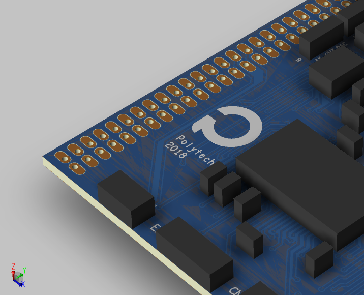
Below is an example of picture rendering after some rework on materials and colors.
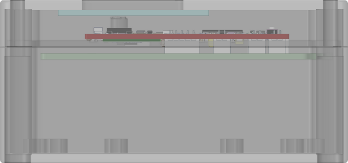
4. Mechanical Integration
Beside producing nice pictures, 3D modeling of electronic boards brings the ability to further take the device design at the mechanical level. Below is an example of board integration (an embedded bird camera) into an off-the-shelf standard box. This model has been designed using the free DesignSpark Mechanical® 3D modeling software.
 |  |  |
- Log in to post comments