
2.4. Part Integration II: PCB footprint
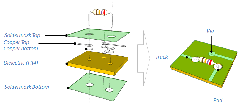
The footprint corresponds to the landing pattern of the physical device onto the printed circuit board (PCB). That's basically a scaled 2D drawing which includes the soldering pads, the device package outline and textual information such as a reference designator (e.g. "R1").
 |  |  | |
| Physical view | Schematic View | PCB footprint (CAD) | PCB footprint (Board) |
Before we start designing footprints, let us review some basic ideas regarding PCBs.
1. Through-hole vs Surface mounted components
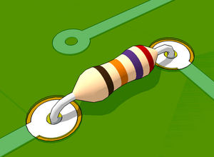
"Through-hole technology (also spelled "thru-hole"), refers to the mounting scheme used for electronic components that involves the use of leads on the components that are inserted into holes drilled in printed circuit boards (PCB) and soldered to pads on the opposite side either by manual assembly (hand placement) or by the use of automated insertion mount machines." https://en.wikipedia.org/wiki/Through-hole_technology
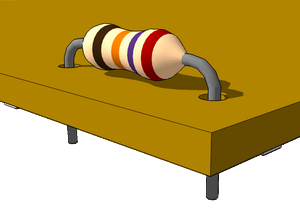
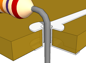
Thru-hole devices are assembled using holes in the printed circuit board. Picture below is an example of a through hole resistor placed on a single-face board. Single-face means that only one layer (usually the bottom layer) holds copper tracks. In such configuration, components are placed on the top surface while soldering is done on the bottom. The solder takes place on the (usually ring-shaped) copper area called the "pad".
 | 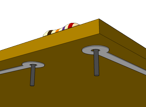 |
| Through-hole resistor (top) | Through-hole resistor (bottom) |
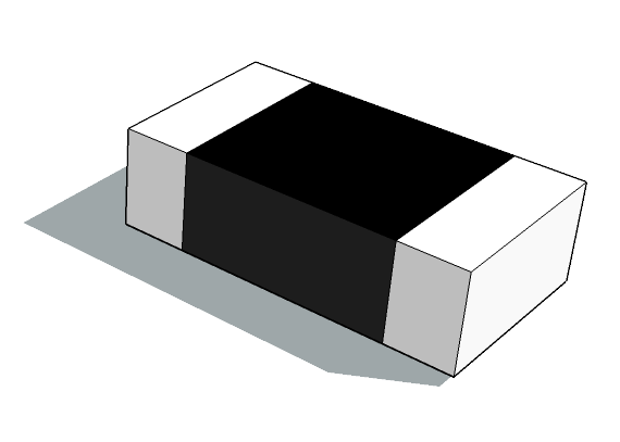
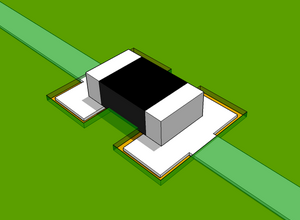
"Surface-mount technology (SMT) is a method in which the components are mounted or placed directly onto the surface of a printed circuit board (PCB). An electronic device so made is called a surface-mount device (SMD). In industry, it has largely replaced the through-hole technology construction method of fitting components with wire leads into holes in the circuit board. Both technologies can be used on the same board, with the through-hole technology used for components not suitable for surface mounting such as large transformers and heat-sinked power semiconductors. By employing SMT, the production process speeds up, but the risk of defects also increases due to component miniaturization and to the denser packing of boards. In those conditions, detection of failures has become critical for any SMT manufacturing process. An SMT component is usually smaller than its through-hole counterpart because it has either smaller leads or no leads at all. It may have short pins or leads of various styles, flat contacts, a matrix of solder balls (BGAs), or terminations on the body of the component." https://en.wikipedia.org/wiki/Surface-mount_technology
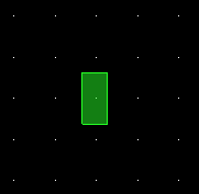
A surface mounted device does not need holes in the board. Here, components and copper tracks are on the same board face. In case of a single-faced board, that would be the top surface. With surface mounted devices, pads are most usually rectangle-shaped.
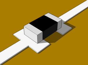 |
| Surface-mounted resistor (top) |
2. Single-faced vs Double-faced board
The previous illustrations show single-face board (with no soldermask layer), such as ones you can easily get from DIY methods (either CNC or chemical etching). It supposes that all the routing is done on a single layer. Such approach is perfectly valid for simple circuits, but becomes quite limited when component and connection count increases. Although using wire straps on the component face (same as 0 Ohm resistors) helps managing unavoidable track crossings, you'll find yourself more at ease using at least 2 routing layers. More layers are also possible (e.g. 4) but requires more expensive industrial processes for fabrication.
Two-layers routing is done on double-faced printed circuit boards, where both the top and the bottom surfaces hold copper tracks. Swapping from top to bottom layer while routing a net can be done at through-hole component locations, or by adding holes having no other purpose than making connections between top and bottom layers. Such holes are called vias. When using both board sides for routing you may also consider placing components on both sides to reduce board area.
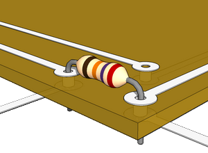 |
| Through-hole resistor on a double-sided PCB |
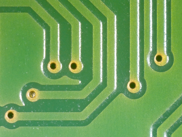
Because vias are used to connect different routing layer, one can guess that the hole is coated (plated) with some conductive material (copper). Be careful, because using rapid prototyping or DIY fabrication method, this is not always true...
 |  |
| Hole without internal coating (non plated hole) | Plated hole |
When holes are not plated, you'll need to make the top-to-bottom connectivity by yourself by soldering through-hole components (or short wires in case of vias) on both surfaces. Again, be careful, because not all component provide easy access to both sides for soldering, especially if you leave no gap between the device and the board. Chemical capacitors are a good example:
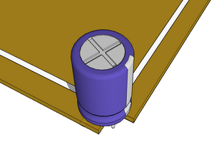 |  |
| Top view of a chemical capacitor placed of the printed circuit board | With no hole plating, top and bottom layers are not connected and soldering on the top surface in not possible unless you leave some gap between the capacitor and the top surface |
Professional printed circuits boards are protected against copper oxidation by means of a finishing varnish (coating) called the soldermask. This coating gives the board its color. The most common (and historical) coating color is green, but you'll find anything now such as blue (arduino), white (nucleo), red (sparkfun boards), ... Some manufacturers add costs when the soldermask in something other than green.
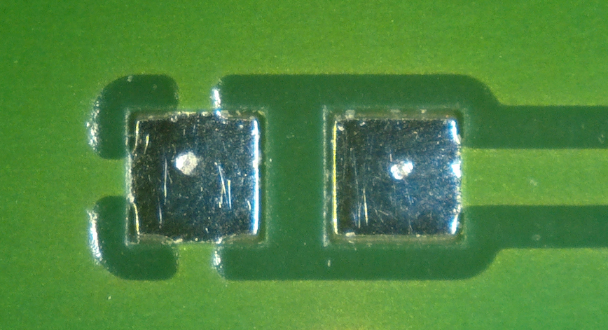
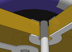
Because coating is a insulating layer, it impossible to solder anything above protected areas. Therefore, the coating must be opened (removed) at locations on top of desired soldering areas (i.e. the pads). You have to define these openings on a specific soldermask layer. Note that vias are left protected since there's nothing to solder there.
 |  |
| Soldermask (green) openings on top of resistors pads. Vias are still protected. | |
 | 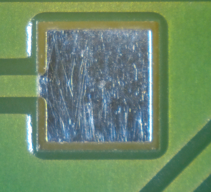 |
| Vias are covered by the protective soldermask coating. | SMD pad with soldermask opening. |
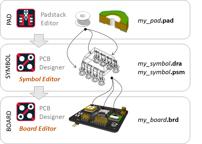
3. Cadence Allegro PCB design flow
Within Cadence Allegro, PCB footprints are called "symbols". What you need to understand is:
A board (.brd file) is an arrangement of symbols (component defined by their footprints) and tracks
A symbol (.dra, .psm files) is an arrangement of pads, a reference designator prefix (e.g. "R1"), and some drawing you may want to help placement (device outlines)
Consequently, regarding the design flow, when you need to integrate a new component, you have to:
Design pads. This is done in the Padstack Editor. You'll end-up with .pad files
Design device symbol (footprint) by placing pads with correct spacing in a 2D working area. This is done in the PCB Editor in Symbol Editing mode. You'll end-up with .dra and .psm files.
Design board by placing symbols and drawing copper tracks. This is done in the PCB Editor in Board Editing mode. You'll end-up with one .brd file. That's your PCB.
4. Pad design
Designing a pad is simple. You basically need to specify the shape and dimensions of the pad and of the soldermask layers.
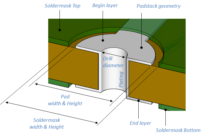
For thru-hole pads, you must provide shape and dimension for the begin layer (top) and the end layer (bottom). You also need to provide a drill diameter.
For SMD pads, you only need to provide begin layer information.
First, you need to find the recommended footprint for your compoment. If you can't, you'll have to measure dimensions on the real device. Going back to our example (STSPIN240 device), we get recommended landing pattern from datasheet. Be careful with units. Both mm and mils are commonly used. Here, we have millimeters.
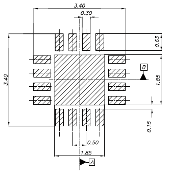
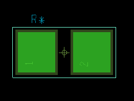
According to this specification, we need to design two pads :
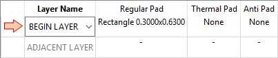
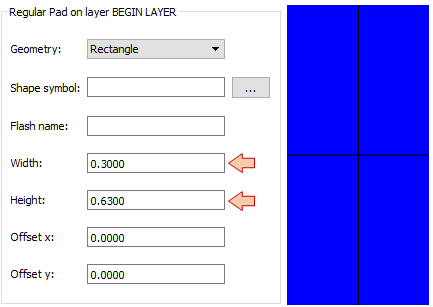
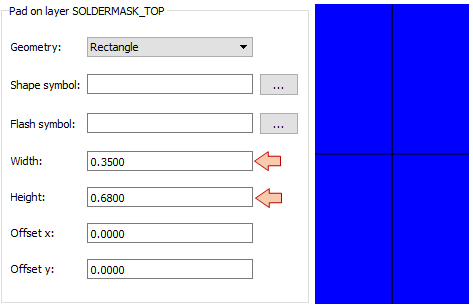
A 0.3mm x 0.63mm rectangle pad that will be used for pins #1 to #16
1.85mm square pad that will be used for the thermal pad (pin #17)
Start the ![]() Padstack Editor Application.
Padstack Editor Application.
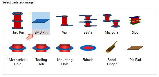
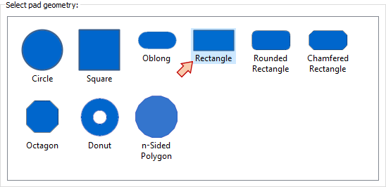
In the Start tab, select SMD Pin and Rectangle geometry:
Make sure units are set to millimeters:
![]()
Now in the Design Layers tab, select BEGIN LAYER and enter the pad dimensions:
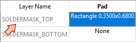
Repeat the above steps in the Mask Layers tab. You should enter dimensions slightly above than those of the pads for the soldermask openings to accommodate alignment error during the fabrication process. As a rule of thumb, you may add about 10% to 20% to both width and height. That would be +5/100 mm here:
When you're done, you can save ![]() the pad file.
the pad file.
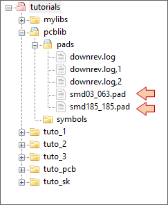
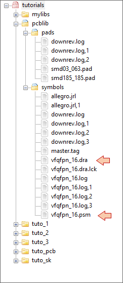
Choose a name you can remember and that identifies the pad definition quite well. Here, I would save this pad under the name "smd03_063.pad" under a tutorials\pcblib\pads\ directory.
Repeat the above steps with the 1.85mm square pad. You may set the soldermask openings to about 1.9mm. Save the pad as "smd185_185.pad". Make sure you have both .pad saved before going on.
5. Footprint Design
Start ![]() Allegro PCB Designer application.
Allegro PCB Designer application.
Select File→New from the main menu.
In the New Drawing dialog:
Make sure that Package symbol is selected as Drawing Type.
Choose a path (e.g. \tutorials\pcblib\symbols\) and a name for the new footprint. The STSPIN240 datasheet specifies that the package belongs to the “Thermally Enhanced Very thin Fine pitch Quad Packages No lead” (VFQFPN) familly with 16 leads (pins). You may then name the foorprint "vfqfpn_16.dra" (or anything you like...). Get used to name the footprint after the package name, rather than after the part name (STSPIN240). Since many different parts share the same package format, chance is that the same footprint can be used for several different parts.
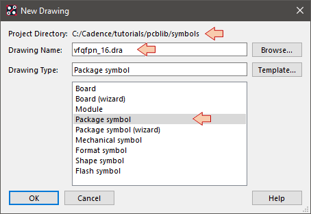
Click OK.
Just like with PCB editing, first step is to configure units and grid.
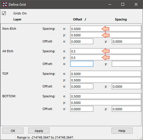
Open Setup→Design Parameters ![]() . In the Design tab choose Millimeters as User units. In the Display tab, click the Setup grids button.
. In the Design tab choose Millimeters as User units. In the Display tab, click the Setup grids button.
According to the STSPIN240 datasheet recommended footprint, pads are 0.5mm pitched, so lets start with a 0.5mm grid. Click OK when done.
Then, you need to make sure that the paths to your pads are well defined in the Allegro environment.
Open Setup→User Preferences...
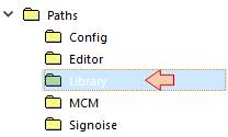
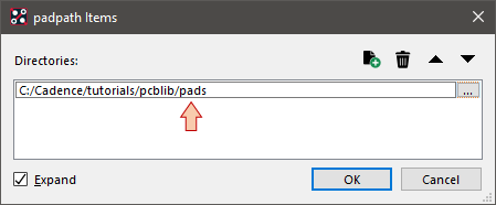
In the Paths/Library category, make sure that the padpath contains the path to the directory you previously saved your .pad files:
When everything looks good, you can quit the user preferences dialogs.
Start placing pads using the ![]() Add Pin button. In the Options side panel click the
Add Pin button. In the Options side panel click the ![]() button beside the Padstack input field. You should be able to browse your .pad directory.
button beside the Padstack input field. You should be able to browse your .pad directory.
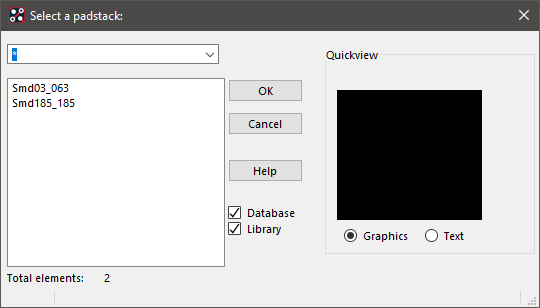
Select the previously saved "smd03_063" pad, leave other options to their default values:
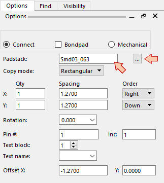
At this moment, you should be ready to place pin #1. Drag the mouse (but do not click) in the working area and you should have a pad attached to the mouse position.
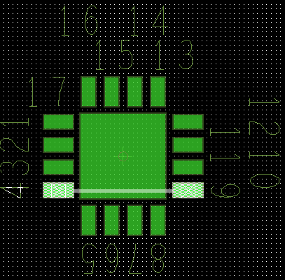
In the Options panel, set the rotation angle to 90° and start placing pins from #1 to #4. according to the STSPIN240 pinout. Pick-up rough location to get a first pin placement. Change the rotation angle along pin placement as needed to place pins #5 to #8 and so on... You may end-up with something like this:
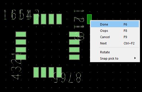
Use the Right-click→Done to exit the Add Pin command.
At this step, you can see that pin numbers are not nicely placed, and much more of a problem that pins are not correctly located each side relatively to each other.
For pin numbers, you can simply pick and drag number as you want:
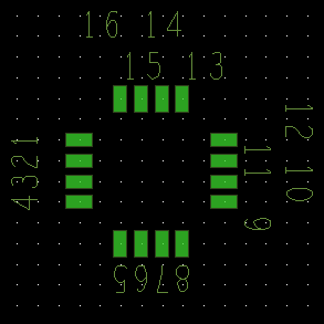
Repeat the above steps and place pin #17, which corresponds to the "smd185_185" padstack:
Then, we need to refine pin placement to exactly match the datasheet footprint. For that may need :
To change grid settings according to your needs
To use editing tools such as the move
 button
To get some help from the lower status bar which displays coordinates:

To toggle from Absolute to Relative coordinates display (status bar A/R button)
To change drawing origin (Setup→Change Drawing Origin)
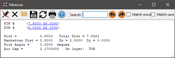
To use the ruler
 to measure distances
That would be very tedious to provide detailed operation. You'll have to experiment for yourself with these tools now. In our example, setting a fine grid pitch to 0.05mm helps a lot moving pins to precise locations.
When done, you should get a symbol with perfectly placed pins. Use the ruler to check that relative distances between pads precisely match those specified in the datasheet. Use the menu entry Setup→Change Drawing Origin to define the symbol origin. You may choose pin #1 or the device geometric center. That's really important because that defines where the mouse-handle will be when placing or moving the component at board level.
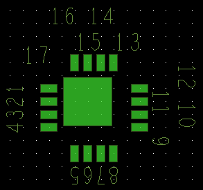
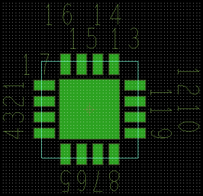
The next step is to draw the package outline. That's not mandatory for a footprint but is something good to have at board level to better work on the device placement. Again, you have to search information in the device datasheet:
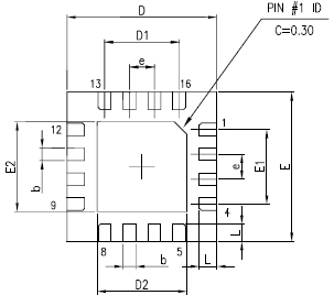
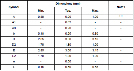
The device package dimensions are provided by D and E dimensions. That's a typical 3mm x 3mm square.
Select the Shape Add Rect tool ![]() . In the Options panel, select Package Geometry / Assembly_Top as the active class/subclass for the drawing layer. Choose Unfilled for the shape filling option:
. In the Options panel, select Package Geometry / Assembly_Top as the active class/subclass for the drawing layer. Choose Unfilled for the shape filling option:
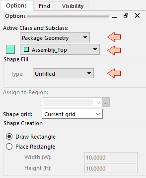
Change the coordinates system to relative and draw a 3mm x 3mm square in the working area. Do not pay attention of exact placement at first.
![]()
Then you may use the moving tool ![]() to precisely center the package geometry with respect to the pad ring:
to precisely center the package geometry with respect to the pad ring:
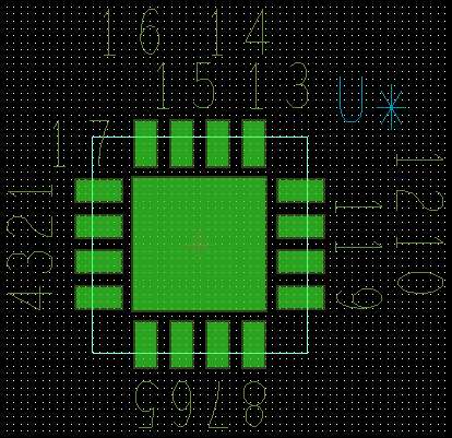
In order to complete the symbol design, you need to add a reference designator. Click the Add Text button ![]() .
.
In the Options panel, select Ref Des as the Active Class:
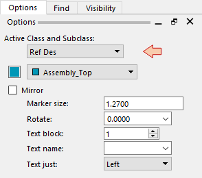
Click in the working area and enter "U*". 'U' is standard for integrated circuits and '*' will be replaced by the instance number when placed at board level (e.g. 'U4').
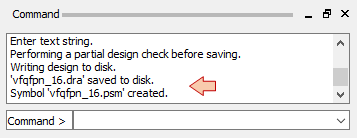
At this step, you should be able to successfully save ![]() the symbol !
the symbol !
Take a look in the log area, you must get confirmation that both .dra and .psm files have been correctly created. If so, then congratulations, you've done your first footprint!
You can now use 'vfqfpn_16' as a PCB Footprint property within Capture.
- Log in to post comments