
1.3. Transient and Frequency Analysis
This tutorial is based on a new schematic. It is recommended to start a new (e.g. 'tuto_2') project, as explained in tutorial 1.1.
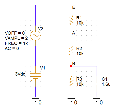
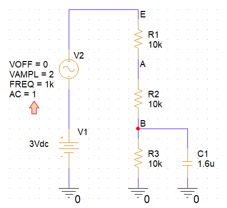
The case study is shown below. Within Capture ![]() , edit the schematic using parts:
, edit the schematic using parts:
R, C from ANALOG library
VDC, VSIN from SOURCE library
1. Bias point Analysis
Save the design and then perform a bias point analysis. Annotate the schematic with simulation results and make sure you've got something similar to the capture below:
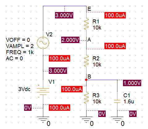
Let us discuss the results from the bias point analysis:
Bias point only considers DC (constant) voltages and currents. Since the sine wave source has no offset, the average DC voltage is 0V. We have $V(E)=V_1+V_2=V_1+0=3V$
$V(A)$ results from $V(E)$ applied to the voltage divider $\frac{R_2+R_3}{R_1+R_2+R_3}=\frac{2}{3}=2V$
$V(B)$ results from $V(E)$ applied to the voltage divider $\frac{R_3}{R_1+R_2+R_3}=\frac{1}{3}=1V$
Because DC (constant) means $\omega=0$, the capacitor impedance $\frac{1}{C\omega}=\infty$. There is no DC current flowing through $C_1$. More generally, you can remove all the capacitors from the schematic when calculating bias point (remove = replace by open circuit)
There's only one DC current loop. The same current flows through all 3 resistors. We can therefore sum up resistors: $I=\frac{V_1}{R_1+R_2+R_3}=\frac{3V}{30k\Omega}=100µA$
2. Transient Simulation
Transient simulation means that x-axis represents time. It basically produces an oscilloscope view of signals. The presence of a sine voltage function generator (i.e. something that varies along time) makes such simulation meaningful. Obviously, when all voltage and currents are constant, there's no point performing a transient simulation.
Create a new simulation profile ![]() and name it 'tran' (or anything you like...)
and name it 'tran' (or anything you like...)
Then take a breath and think!
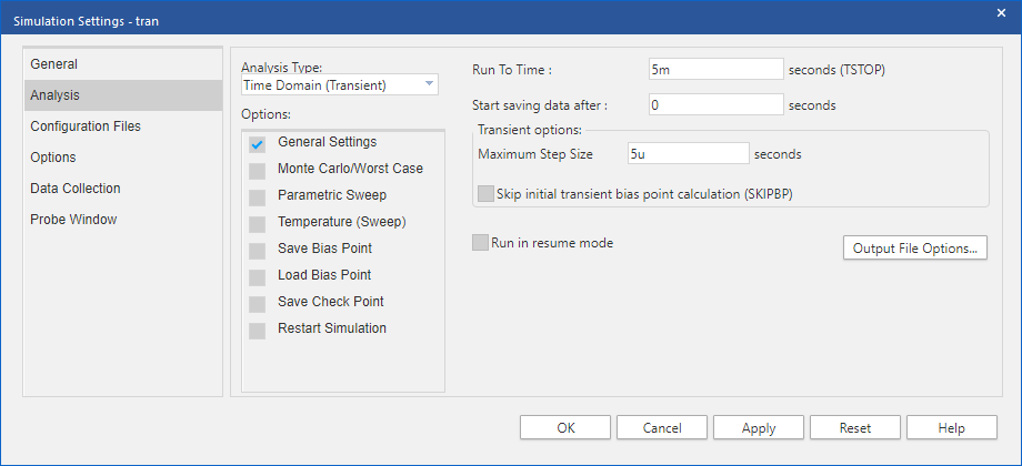
Transient simulations may produce large amount of data (disk space) if you want to calculate data for long. It is advised to restrict the simulated time to something reasonable. Here, we have a 1kHz sine wave. One signal period is 1ms. Simulation over 5 periods should be good enough to see something. So let's limit the final time to 5ms (TSTOP).
Next, you can limit the maximum step size if you want smooth simulation results. This is optional, and you may leave that field empty. The 5µs setting below guaranties that a minium of 1000 points (5m/5u) will be produced in the simulation result. Again, be careful... the smaller the maximum step size is, the more data you'll get onto your drive space.
Save the settings and launch ![]() the transient simulation. When it is done, in the
the transient simulation. When it is done, in the ![]() PSpice result window add the following traces
PSpice result window add the following traces ![]() to the plot:
to the plot:
$V(E)$
$V(A)$
$V(B)$
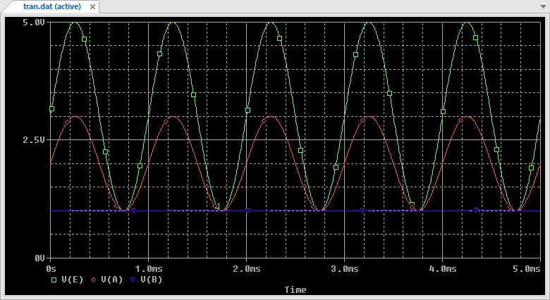
Some comments on the above results:
First look at the average values (offsets) of each signal. We retrieve the previously calculated bias point : $V(E)=3V$, $V(A)=2V$, $V(B)=1V$
Next, you might be surprised by the $V(B)$ signal in which the sine wave disappeared, leaving the signal plot almost flat. Because we're now applying an harmonic input, one should consider the effect of $C_1$. For 1kHz signal frequency, the impedance module of $C_1$ is given by $|Z_{C1}|=\frac{1}{C\omega}=\frac{1}{2\pi fC}=\frac{1}{2\pi\times1000\times1.6 10^{-6}}=99\Omega$ With $R_3$ parallel to $C_1$, the equivalent impedance of the bottom stage is now 98.5$\Omega$. In such situation, one would say that for 1KHz signal frequency "$C_1$ is bypassing $R_3$" (i.e. C1 is a shortcut across R3). Does that means that node B is simply "grounded"? Well, yes, and no... Let's consider the following:
According to bias point results, $V(B)=1V$, so node B is clearly not DC grounded
Even for 1kHz signal, node B is tied to ground through a 98.5$\Omega$ resistor. Such resistance is not a true shortcut
Yet, $V(B)$ is now constant. A small-signal mass hypothesis at node B is therefore very tempting! And quite legit considering the resistance ratio between $R_1+R_2$ resistors (20k$\Omega$) and the $C_1$ impedance ($<100\Omega$) for frequencies above 1kHz.
Accepting the above assumption of a small-signal mass at node B, you'll understand that amplitude of $V(A)=1V$ is half the one of $V(E)=2V$ due to the voltage divider $\frac{R_2}{R_1+R_2}$
3. Frequency Analysis
Frequency analysis is used to study the frequency response of the circuit. Up to now, we only considered two points:
f=0 (bias point)
f=1kHz (transient simulation)
Spice frequency analysis is called AC Analysis. It requires that you specify at least one AC source in your netlist. Usually, AC source is the voltage source associated with input signal. A common practice is to set the AC source magnitude to 1V. Doing so, output level may be considered as gain as well:
$\frac{V_{out}}{V_{in}} = V_{out}$ when $V_{in}=1$
Even if this is beyond the scope of this tutorial, you may note that amplitude level in AC analysis is barely an issue because the simulated circuit is linearized (small-signal equivalent model) before the simulation is performed.
Change the AC value of V2 voltage source to 1V as shown below:
Create a new simulation profile ![]() and name it 'ac' (or anything you like...)
and name it 'ac' (or anything you like...)

Then set the frequency range you want to cover. X-axis of a Bode diagram represent the frequency on a logarithmic scale. The below settings cover frequencies from 10mHz to 100kHz with 100 points per decade for smooth tracing:
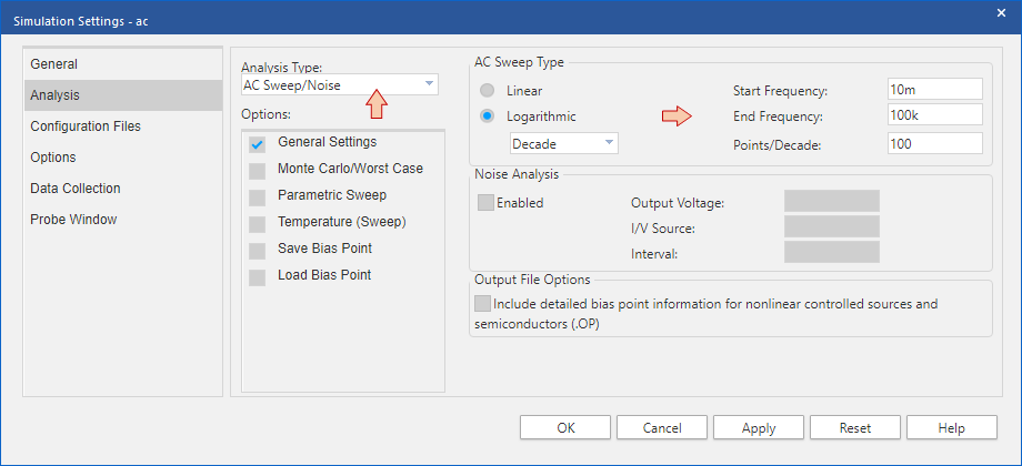
Apply the above settings and then run ![]() the AC analysis. When simulation is done, add the following traces
the AC analysis. When simulation is done, add the following traces ![]() to the plot again:
to the plot again:
$V(E)$
$V(A)$
$V(B)$
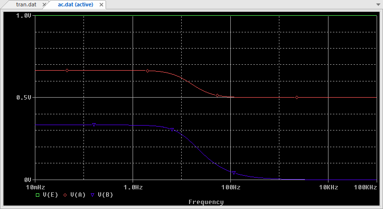
Let us analyze the results:
AC means harmonic (sinusoidal) input signal. In the above plot, DC would be represented at $f=0$, therefore infinitely far in the left direction of the plot. Yet, analyzing very low frequencies (down to 10mHz here) and given that signals exhibits a quite stable level up to 1Hz, one can consider that left end of the plot is representative of the DC behavior of the circuit:
$V(E)=1V$ → Amplitude of $V(E)$ is the same as amplitude of input source (AC=1V). From the biasing point, we had $V(E)=3V=V_1$
$V(A)=\frac{2}{3}$ → Amplitude of $V(A)$ is $\frac{2}{3}$ that of the input source. From the biasing point, we had $V(A)=2V=V_1\times\frac{2}{3}$
$V(B)=\frac{1}{3}$ → Amplitude of $V(B)$ is $\frac{1}{3}$ that of the input source. From the biasing point, we had $V(B)=1V=V_1\times\frac{1}{3}$
On the right end of the plot, frequency is high, therefore the assumption that $C_1$ impedance is very low is strong enough to consider $C_1$ as a shortcut:
$V(E)=1V$ → $V(E)$ is not affected by $C_1$ because $V(E)$ is directly connected to the input source. In the transient simulation, you can see that $V(E)$ amplitude is 2V, same as the input source.
$V(A)=0.5V$ → Amplitude of $V(A)$ is half that of the source. We already observed that in the transient simulation
$V(B)=0V$ → Amplitude of $V(B)$ is zero. Again, this is déjà vu in the transient simulation
Finaly, the middle of the plot reveals the effect of $C_1$ state, changing from an "open circuit" (at low frequencies) to a "short circuit" (at high frequencies). Of course, saying so is totally inaccurate since $C_1$ impedance evolves continuously and smoothly when frequency increases ($|Z_{C1}|=\frac{1}{C\omega}$). Still, one can observe particular frequencies in the vicinity of 10Hz, where important changes seem to occur. These singular frequencies are poles and zeroes in the transfer functions $H_A(p)=\frac{V_A}{V_{in}}$ and $H_B(p)=\frac{V_B}{V_{in}}$. These frequencies do not only depends on $C_1$ impedance, but on the interaction of $C_1$ with surrounding resistors. Assuming $R_1=R_2=R_3=R$ and $C_1=C$, we have:
$H_A(p)=\frac{R+(R//C)}{2R+(R//C)} = \frac{2}{3}\times\frac{(1+\frac{1}{2}RCp)}{(1+\frac{2}{3}RCp)}$
$H_B(p)=\frac{(R//C)}{2R+(R//C)}= \frac{1}{3}\times\frac{1}{(1+\frac{2}{3}RCp)}$
$f_{pole} = \frac{1}{2\pi\frac{2}{3}RC} \approx 15Hz$
$f_{zero} = \frac{1}{2\pi\frac{1}{2}RC} \approx 20Hz$
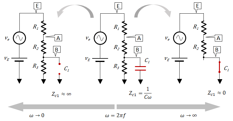
The figure below illustrate the two equivalent circuits we obtain at both very low and very high frequencies based on the capacitor impedance approximations.
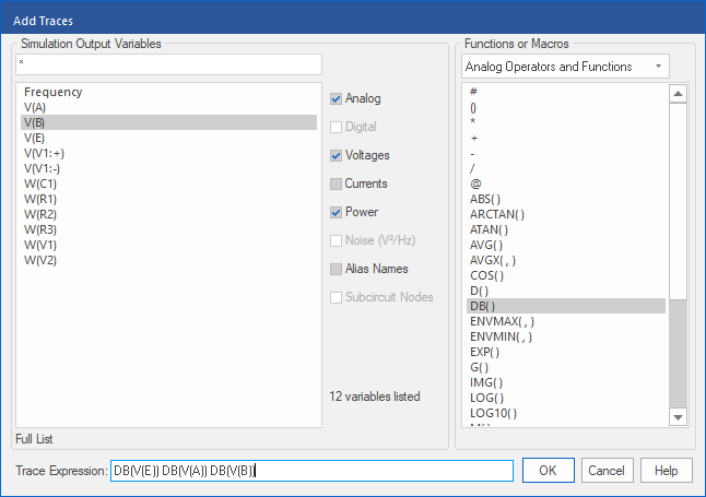
For now, delete all the traces from the plot and click the Add Trace button ![]() again. Instead of plotting $V(E)$, $V(A)$ and $V(B)$ amplitude, let's plot gains in dB unit. Click the DB() operator and then the Output variable $V(E)$ to build expression as shown below:
again. Instead of plotting $V(E)$, $V(A)$ and $V(B)$ amplitude, let's plot gains in dB unit. Click the DB() operator and then the Output variable $V(E)$ to build expression as shown below:
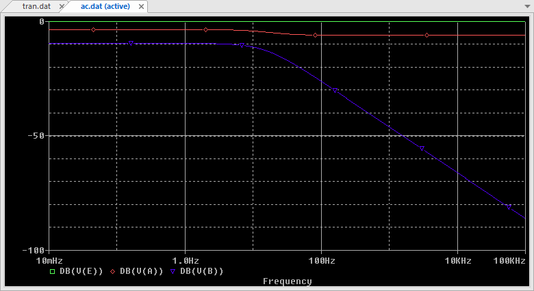
That's closer to a Bode diagram:
Let's now focus on $V(B)$. Again, clear all trace from the plot, then add a second plot to the window using main menu Plot→Add Plot to Window. Then add the following trace expression:
$DB(V(B))$ in the top plot (magnitude in dB)
$P(V(B))$ in the bottom plot (phase in degree)
That's a Bode diagram!
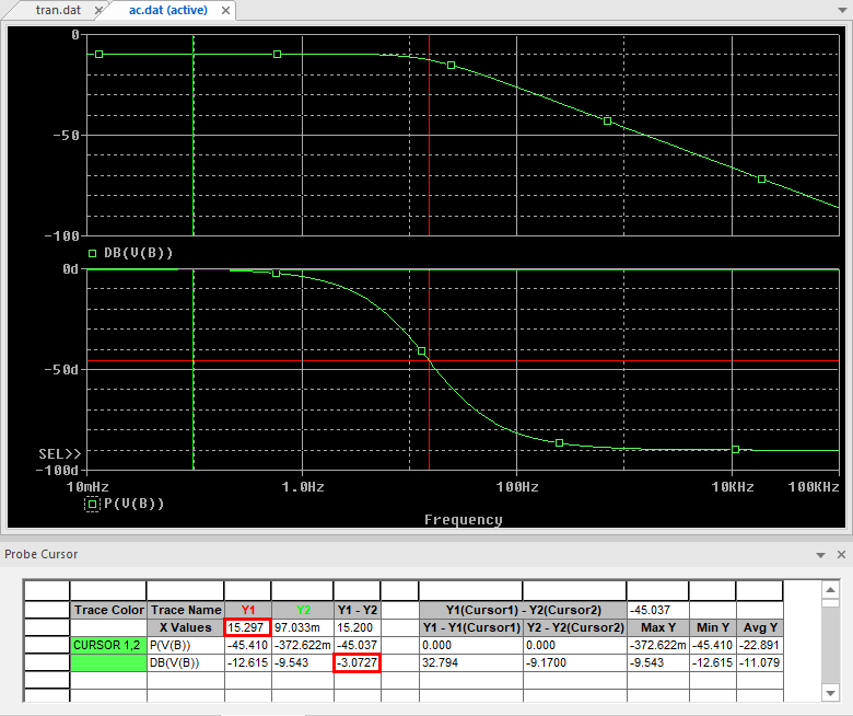
You can use cursors ![]() as shown above to measure the -3dB cutoff frequency of $H_B(p)$ on the magnitude plot.
as shown above to measure the -3dB cutoff frequency of $H_B(p)$ on the magnitude plot.
X(Y1) = 15Hz @ DB(Y1-Y2)=-3dB → That's a perfect match with pole frequency calculated above!
- Log in to post comments