
2.1. Introduction to PCB Design
This tutorial is for complete beginners with Cadence SPB board design environment. It is a step-by-step guide through the design of a PCB for a basic amplifier stage. PCB design is always under the control of a netlist, that is to say a schematic.
Therefore, the main steps leading to PCB design include:
- Preparing an electronic schematic of the circuit you want to turn into a board
- Preparing (or collecting) PCB footprints for all the physical devices in the schematic
- Performing part symbols and PCB footprint association
- Generating the schematic netlist
- Placing parts (location, orientation) onto the board surface
- Tracing copper routes between parts
1. Preparing the Schematic
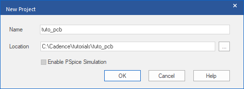
At first, you'll need to create a new project ('tuto_pcb' for instance) under ![]() Cadence Capture CIS.
Cadence Capture CIS.
Then edit the full schematic as shown below:
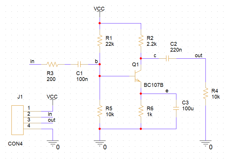
Spice simulation is not involved here, you may therefore use parts from any library. For this design, you can use parts from these libraries:
| Reference | Part Name | Library |
| R1, R2, R3, R4, R5, R6 | R | library/pspice/analog.olb |
| C1, C2, C3 | C | library/pspice/analog.olb |
| Q1 | BC107B | library/pspice/ebipolar.olb |
| J1 | CON4 | library/connector.olb |
A printed circuit board is a real physical thing. Therefore, you can only place real components. For instance, you can't place functional parts such as power sources that we use for simulation. Every outboard stuff you want to further connect to the circuit (power supply lines, input and output signals, ...) will access the PCB components via physical connectors (J1 here).
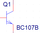
Once the schematic is done, the next step is to specify a footprint for each part. The footprint is a drawing which defines the component landing pattern (pads type and position) for the soldering and additional information such as part outline, pin numbering and reference designator.
 | 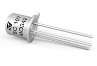 | 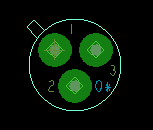 |
| Schematic view | Real thing (TO18 package) | TO18 Footprint |
2. Collecting and associating footprints
Within Cadence Allegro, footprints are stored as .dra files. A footprint file instantiates pads. A pad defines the soldering copper surface (ring, oblong, rectangle...), and optionally the drill for through hole mounting components. Pads are defined and stored separately in .pad files, but you need to understand that a footprint file (.dra) requires its associated pad files (.pad).
Footprint design out of the scope of this tutorial. For now, you can download a small archive with the required footprints here.
Unzip the file tutolib.zip and store the tutolib\ folder and its content (pads\ and symbols\ folders) somewhere on your drive you can remember. There's five footprints in the archive you'll need to associate as follow:
| Reference | Footprint name |
| R1, R2, R3, R4, R5, R6 | res_01 |
| C1, C2 | cap_02 |
| C3 | cap_03 |
| Q1 | to18 |
| J1 | con_04 |
Footprint association is pretty simple. Double-click a part in the schematic to open the part properties tab. Then enter the name of the footprint file you want to associate (without .dra extension) in the PCB Footprint property field.
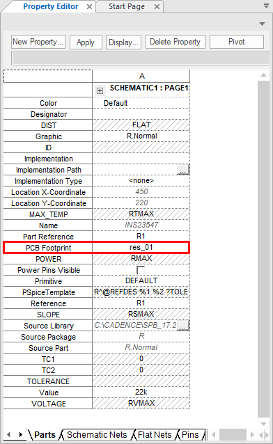
Save ![]() the properties when done.
the properties when done.
Repeat the above operation for all parts in the schematic, using the above table.
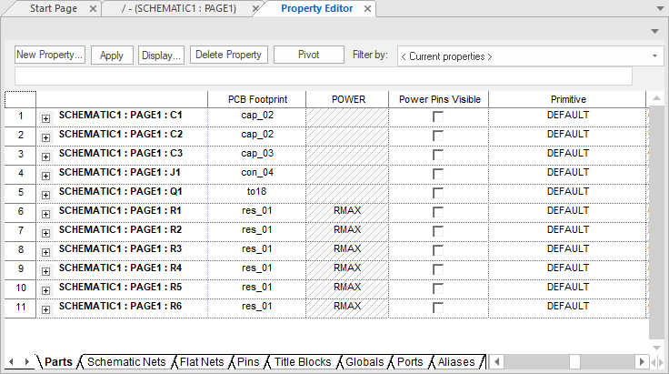
If you find this tedious, you can also select all parts in the schematic (CTRL-A), then press ENTER to open properties tab for all parts altogether. You can filter properties class by using the Allegro PCB Designer filter on top of the area. Then playing with Pivot button, you can achieve the arrangement below and enter footprint names in a much convenient way (including copying cells by mouse drag). It's also a good way to make sure nothing is left apart.
Save ![]() before closing!
before closing!
By now, the schematic is ready for PCB design. But before exporting the netlist into PCB Designer tool, there is something we need to do.
Make sure everything is saved and close the ![]() Capture application. We'll need a fresh restart after the library path settings we'll do next.
Capture application. We'll need a fresh restart after the library path settings we'll do next.
3. Preparing PCB Designer
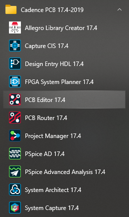
From Windows® start menu, launch ![]() PCB Editor (under Cadence Release 17.2 folder)
PCB Editor (under Cadence Release 17.2 folder)
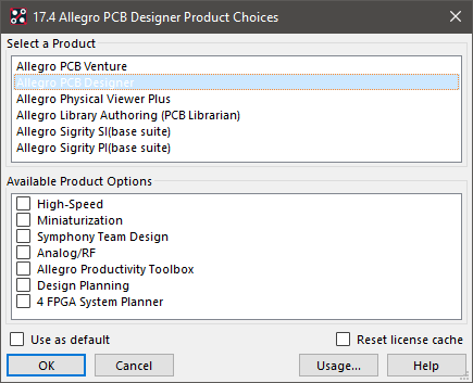
Then select Allegro PCB Designer license and click OK:
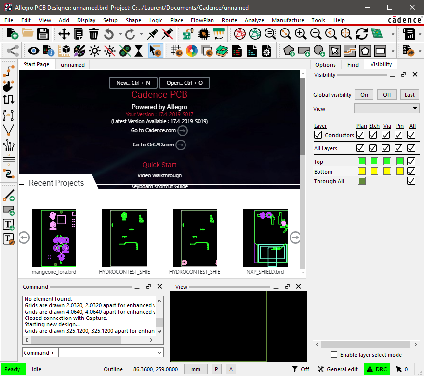
The Cadence Allegro PCB design environment opens:
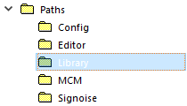
From the main menu, select Setup→User Preferences...
Then, in the Categories area, expand the Path folder, and select Library item:
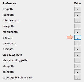
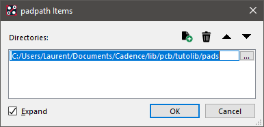
We need to setup PCB editor with paths to our footprint library (the tutolib folder, you've downloaded earlier). Click on the Value button in front of padpath preference:
Using the ![]() and
and ![]() buttons, remove all existing paths, and add a new path corresponding to the pads\ folder of tutolib (use your own path):
buttons, remove all existing paths, and add a new path corresponding to the pads\ folder of tutolib (use your own path):
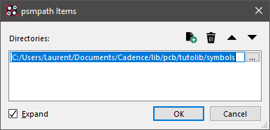
Repeat the above operations with psmpath preference, now using the path to the symbol\ folder:
You can now click OK to close the User Preferences window, and quit the PCB editor. It's ready for the next operation...
4. Exporting the Schematic into the PCB Editor
Relaunch ![]() Capture and reopen the 'tuto_pcb' project.
Capture and reopen the 'tuto_pcb' project.
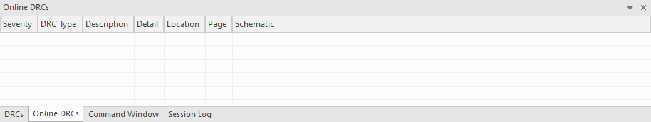
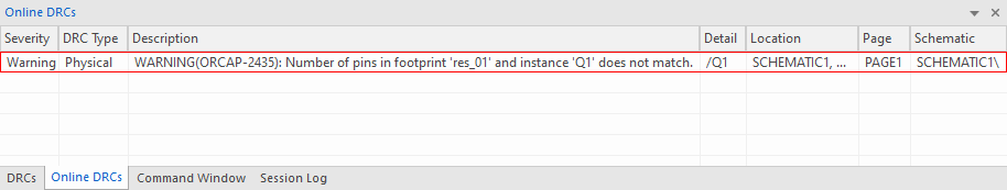
Take some time to look at the Online DRCs frame. DRC stands for 'Design Rules Check'. Capture performs some real-time verifications as a background task while you're working on the schematic, and may warn you if design exhibits inconsistencies. This list must be empty... If not, then you have some stuff to repair.
Try to change the transistor PCB footprint for instance, using the 'res_01' footprint instead of the required 'to18':
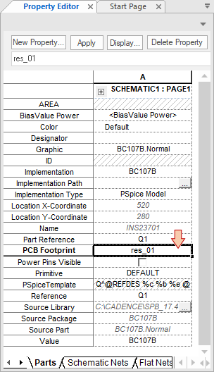
Save the properties and watch out the Online DRCs. You get a pretty explicit warning that reports a mismatching pin number between the transistor symbol (3 pins) and the res_01 footprint (2 pins):
Repair any warning you may find here. There's no point going further as long as you have any problem in the schematic.
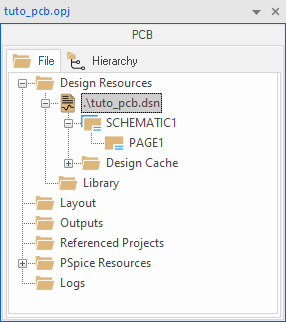
When all clean, select the main design resource tuto_pcb.dsn in the project tab:
Make sure the project is saved (right-click → Save), and then from the main menu select Tools→Create Netlist... or click ![]()
You can leave options as proposed and click OK.
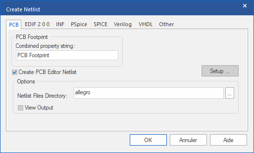
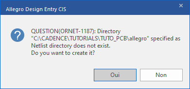
You'll be asked to allow folder creation, just say Yes. The allegro\ subfolder will be used to store a (big) number of files associated with PCB design.
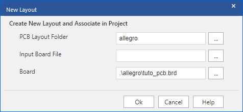
Then from the main menu, select PCB → New Layout. Since there is no existing layout already, leave the Input Board File field empty. Leaving this field empty means that the board file ('tuto_pcb.brd') will be initialized with no previous design, and hence let you start from scratch. If you need to create or resume a new layout based on an existing one, you may provide something here.
Clicking OK here launch a process that:
Performs a complete check of the design
Verifies footprints availability and consistency (pin numbers and names matching for each part between schematic symbol and PCB footprint)
Starts the PCB Editor with schematic netlist loaded
Let's go!
Then watch out! A progress window appears for a short time, indicating success or failure of sequential operations. When finished, if everything went fine, the log area should report this:
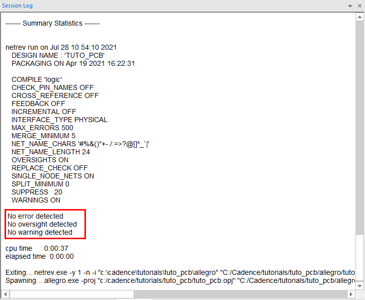
If you have anything wrong (errors or warnings) DO NOT GO FURTHER. That's useless because even small warnings will most likely produce missing footprints later on at PCB stage. Instead, scroll up the log and find out what's wrong. Then fix problems and start the create netlist operation over until you get no errors and no warnings.
If log report is clean, you can select the Allegro PCB Designer license again and wait until the ![]() Allegro PCB Designer environment opens. Then you can start working on the PCB.
Allegro PCB Designer environment opens. Then you can start working on the PCB.
5. PCB Designer Settings
Make sure the grid is on by using the ![]() button.
button.
Next select Setup→Design Parameters... from the main menu or click the ![]() button.
button.
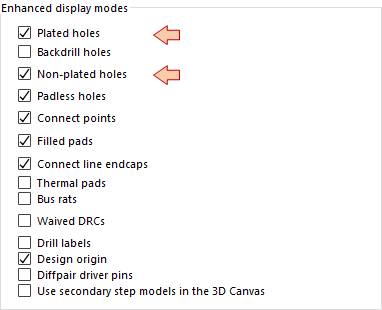
In the Display tab, enable the display of Plated holes and Non-plated holes and leave other options as proposed
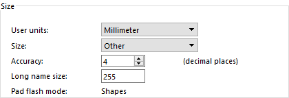
In the Design tab, change units to Millimeters (you may get a warning dialog box regarding accuracy, just click OK). Click the Apply button at the bottom of the window to apply unit changes before next step
Come back to the Display tab, and click the Setup grids button
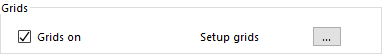
Set the grid spacing to 1.27mm everywhere. That spacing corresponds to half 2.54mm, which is the standard (labdec) pin spacing for several through hole components. Then click OK.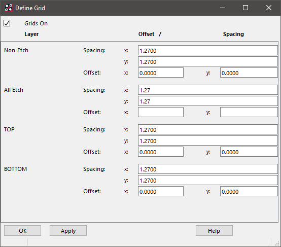
You finally can close the Design Parameters window by clicking OK. Back the the main editor working area, you may adjust the zooming using mouse wheel.
6. Part Placement
From the main menu, go to Place→Manually... or click the ![]() button. The Placement window opens:
button. The Placement window opens:
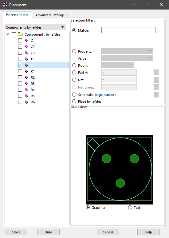
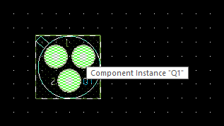
Select the transistor part Q1, then hover the mouse outside the Placement window in the working area. You should see the Q1 footprint attached to the mouse cursor. Click anywhere you like to place Q1. Observe that Q1 is now flagged as placed in the part tree view.
Repeat the above operation for all parts. Use the schematic topology to get a rough initial placement. Indeed, placement should be done carefully, keeping in mind future routing. For instance, try to keep two connected parts as close as possible from each other.
You can rotate parts while placing using right-click to invoke contextual menu and then Rotate. It will take some time to understand how PCB editor manage commands. While you are in an interactive command (placing and rotating components for now), you can access live options using the right pane. Here you can for instance change the rotation angle (default is 90°).
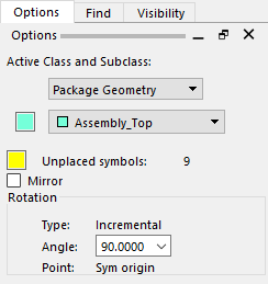
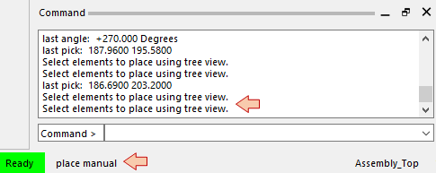
Be careful with the Mirror function... Mirroring a component consist in placing the component on the opposite side of the board. We do not want this here, all components being placed on the top-side of the board. While in an interactive command, Cadence provide instructions in the command area, and you must monitor the current state in the bottom status bar:
When you are done placing components, you must quit the place command using a right-click somewhere in the working area, and then Done. This is an habit you need to get used to as it is the way to terminate pretty much every command within Allegro.
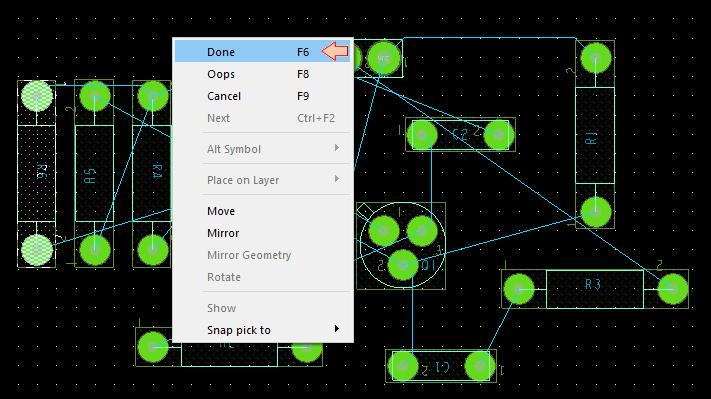
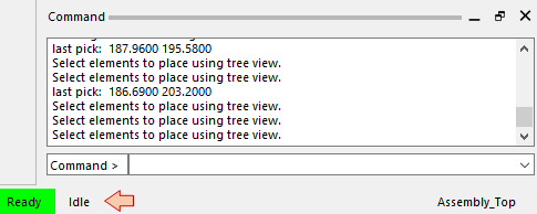
Make sure the command is no more active by a glance to the status bar indicating Idle. Idle is the status you should have before starting any new operation.
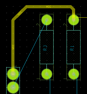
When you're done placing/rotating all the components, you may end up with something similar to this:
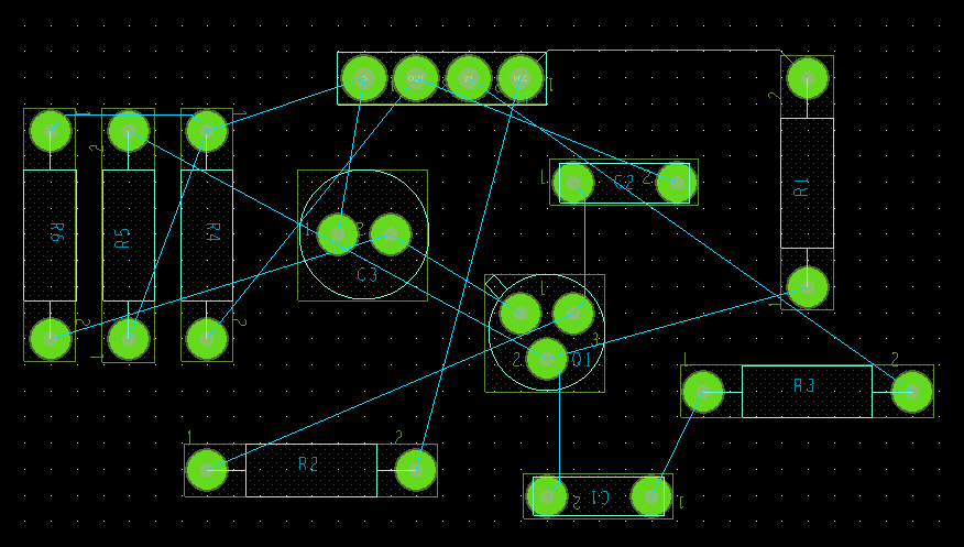
Note that initial placement we've done is something quite random. The blue lines connecting symbols are called 'rats'. These are not copper tracks. It just shows logical connections between components. It is a placement help. Shorter rats, with few crossings will make the routing more straightforward. As you can see, we have room to make it better...
Time has come to refine placement. For that, let us use colors for rats to help focus on priorities.
Click the Color/Visibility ![]() button, then select the Nets tab. Using the color palette, change net 0 (ground) rats color to dark gray, and Vcc net rats to yellow:
button, then select the Nets tab. Using the color palette, change net 0 (ground) rats color to dark gray, and Vcc net rats to yellow:
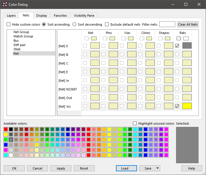
Click Apply and then OK.

Use the move/rotate ![]() button to refine placement. Forget about ground rat (net 0) for the moment, as ground routing will be processed using a ground plane when all other routing is complete. Concentrate on signal rats (blue) and Vcc rat (yellow). Try to arrange components nicely (close to each other but not too much, aligned, and avoiding too much rats crossings). Now it's art!
button to refine placement. Forget about ground rat (net 0) for the moment, as ground routing will be processed using a ground plane when all other routing is complete. Concentrate on signal rats (blue) and Vcc rat (yellow). Try to arrange components nicely (close to each other but not too much, aligned, and avoiding too much rats crossings). Now it's art!
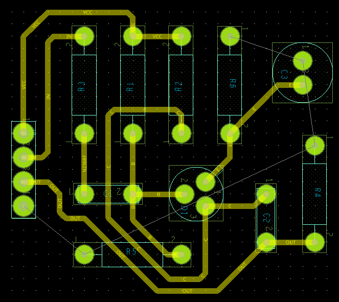
Here is an example of refined placement:
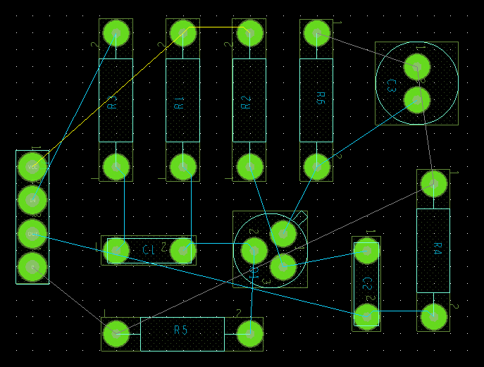
Be aware that you can't really know if the placement will work until you've done routing (drawing copper tracks). You can only gamble on success... Be prepared to move parts again while routing...
7. Routing
7.1. The Constraint Manager
Before starting to draw copper track, we need to tune something called the Constraint Manager. Constraints are a set of physical rules (track width, distance between tracks, between pads, ...) that Allegro uses to produce warnings when a rule is violated while drawing. Constraint are defined depending on your PCB provider manufacturing capability, and targeted board price (the smaller patterns, the more expensive). There are hundreds of rules you can specify in the constraint manager, but we'll only set a few for this tutorial.
Open the constraint manager ![]() .
.
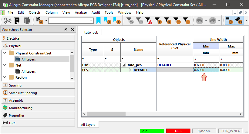
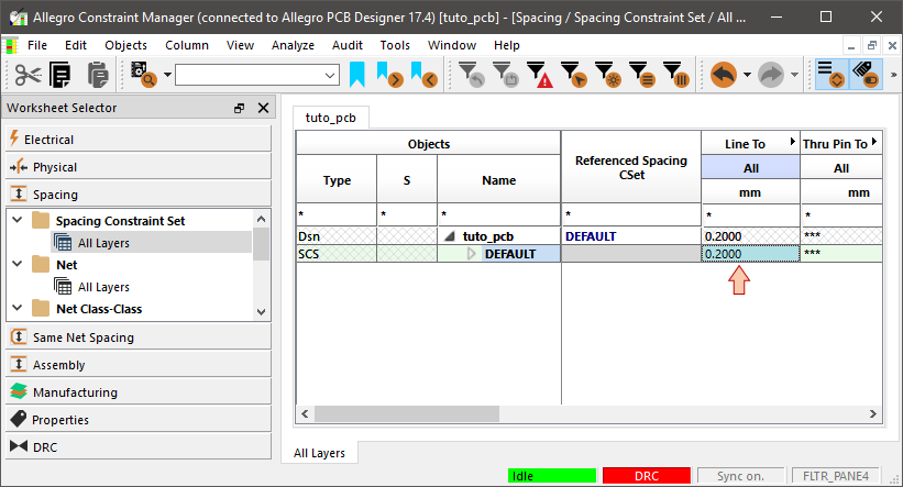
In the left pane, open the Physical section and select All Layers under Physical Constraint Set. Then change the minimal Line Width to 0.6mm:
In the Spacing section, change the Line to All spacing to 0.2mm:
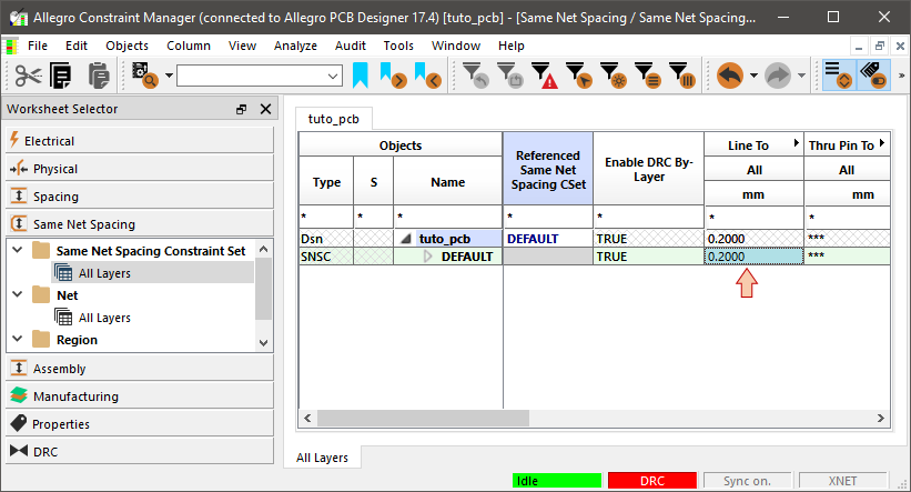
Repeat the above setting in the Same Net Spacing section:
That should be enough to get started, so you can close the Constraint Manager window.
7.2. Net Routing
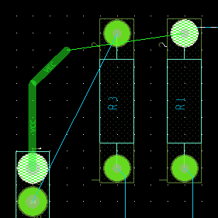
Hit the Add Connect ![]() button and than click on J1 upper pad. You're drawing a copper track:
button and than click on J1 upper pad. You're drawing a copper track:
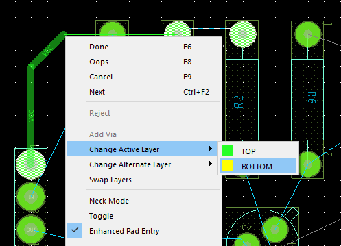
The green color is the default color for tracks on the top side of the board. Since we're routing through-hole components, we'd rather route on the bottom side. Invoke the contextual menu while routing and change the active layer to Bottom:
Then keep going:
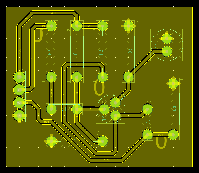
Use rats to connect all the components repeating the above operation. An example of completed routing (except for the ground net) is shown below:
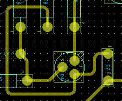
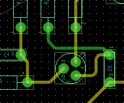
It would be very tedious to explain all the editor functionalities in this tutorial... You'll have to experience by yourself some editing tools:
You can shift
 or delete
  existing tracks
You can change track width (a track with different widths is possible) using the contextual menu while routing
You can move part with tracks keeping their attachment (Options→Slide Etch while moving)
Note that all signals have been routed on the bottom side of the board here. That's often possible with simple circuits with few components. With more complex circuits, you'll need both sides of the board to manage net crossings or avoid long tracks. For instance:
 |  |
| Single-side routing | Double-side routing |
In this tutorial, let-us keep the routing single-face.
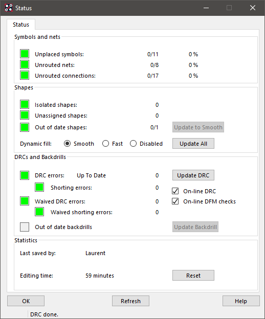
When done, from the main menu select Display→Status. You may click the Update DRC button to get something similar to this:
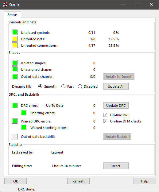
This dialog box is very important. It states that all symbols (components) are placed, which is good, but also reports that one net with four connection is still to be routed. You may click the tiny yellow button Unrouted Connections to get detail:
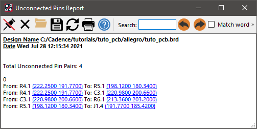
As expected, we still need to route ground net. But this one will be processed using a ground plane instead of tracks.
7.3. Ground Plane
Before getting into ground plane design, we need to define the board outline (shape and dimensions).
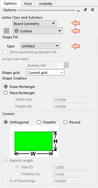
Click the Shape Add Rect ![]() button, then focus on the Options right pane. Select Board Geometry and Outline as Class/Subclass and make sure that Shape Fill Type is Unfilled:
button, then focus on the Options right pane. Select Board Geometry and Outline as Class/Subclass and make sure that Shape Fill Type is Unfilled:
Then draw a rectangle encompassing the whole routed area by clicking two opposite corners. Use the contextual Done when finished:
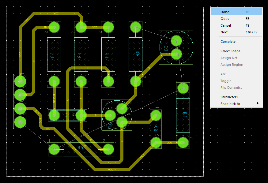
This rectangle defines the board limit. We'll use this to draw the ground plane as well.
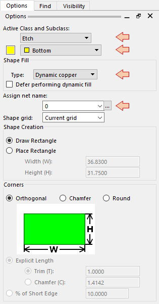
Click the Shape Add Rect ![]() button again, and again focus on the Options right pane. Select Etch and Bottom as Class/Subclass. This time we want the shape to be copper plane, on the bottom side of the board. Make sure that Shape Fill Type is Dynamic Copper, and assign net 0 to the shape using the ... button.
button again, and again focus on the Options right pane. Select Etch and Bottom as Class/Subclass. This time we want the shape to be copper plane, on the bottom side of the board. Make sure that Shape Fill Type is Dynamic Copper, and assign net 0 to the shape using the ... button.
Then again, click on two opposite corners to draw the ground plane rectangle, using the same dimensions as for the board outline:
Congratulation, your PCB is now completed and ready for fabrication. You may check the status: All green!
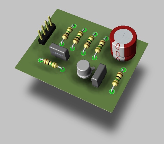
Allegro 3D rendering of the finished board (requires a STEP 3D model for each part). See tutorial 2.7 if you're interested.
- Log in to post comments