
2.2. Other things to know with PCB Designer
This chapter covers specific operations you'll need when designing a PCB. It is a follow up of the previous introduction to PCB designer and relies on the same amplifier circuit project (tuto_pcb).
If not already opened:
start
 Cadence Capture and open the 'tuto_pcb' project.
From Capture main toolbar, click the
 Open Active Layout button.
You should have both schematic and PCB opened and synchronized at this moment.
In this tutorial, you'll learn:
To update an existing PCB after minor changes in the schematic
To use vias and double-side routing (or multi-ayer routing)
To tune ground plane thermal reliefs
To setup and add text
1. Updating an existing PCB after a change in the Schematic
This is a very common situation while designing a PCB: You've done a lot of work placing components and editing tracks and then you need to change something at the schematic level, such as:
Adding or removing a component
Fixing a wiring error
Swapping pins on a connector to ease final routing when the connector pinout is not constrained (very common).
In such cases of small schematic adjustments, that would be a nightmare to start over the whole place and route process. Let see how to do that with minimal damage.
In Capture, edit the schematic to reflect changes you want. Let us for instance shift down in and out signals on the connector to move GND close to VCC:
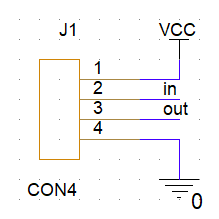
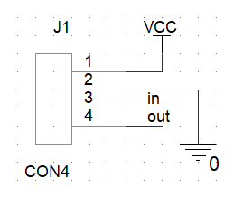
Before After Save the design. At this moment, the PCB layout is no more in sync with the schematic. You can perform synchronization operations both ways using menu buttons:
- Update Layout
- Update Schematic
Click the Update Layout button. Review the changes that are summarized in the Update Layout dialog: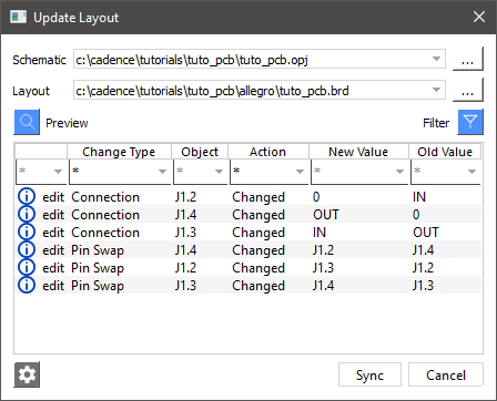
Click Sync if you're OK while watching the Command log in the PCB Designer window. You should see the Sync operation to be received and executed on the PCB side: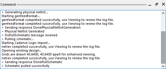
Review the PCB with the new netlist. Your previous routing work is unchanged, but because the netlist is now updated, there will be obvious errors and probably new rats showing missing connections. Clean-up the area by deleting obsolete track segments, and then re-route correct nets.
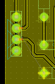
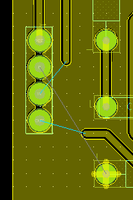
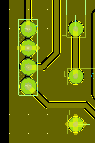
DRC errors and new rats have appeared Delete faulty segments to get a clearer
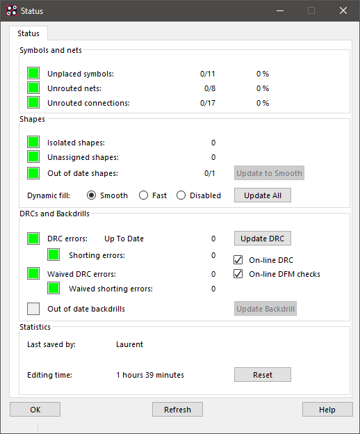
view of what you have to toDraw new tracks When you're done applying corrections, check the PCB status and make sure all is green. You're done.
2. Double-side routing
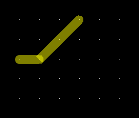
Double-side routing is pretty standard. In the previous tutorial, only single-side routing was considered. For double-side routing, you'll need to define vias. A via is a particular padstack (hole and rings) which purpose is to travel from one side to the other while routing a connection.
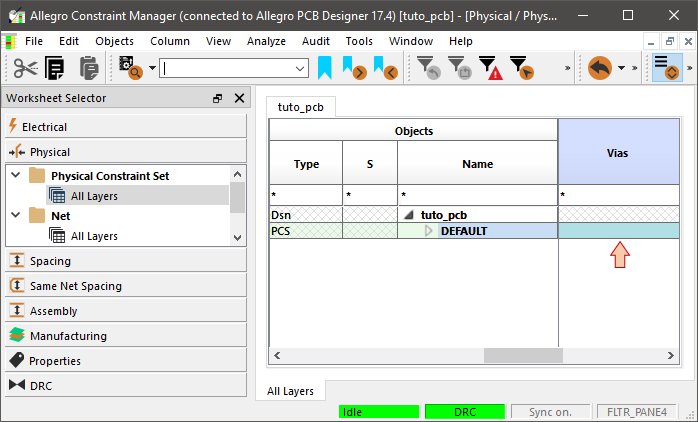
Open the constraints manager ![]() . Expand the Physical category and select All Layers under Physical Constraint Set. Scroll horizontally in the spreadsheet to locate the Vias column, then click in the empty cell.
. Expand the Physical category and select All Layers under Physical Constraint Set. Scroll horizontally in the spreadsheet to locate the Vias column, then click in the empty cell.
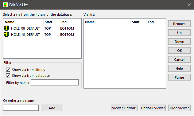
The Edit Via List dialog opens. Our tiny library only contains two pad stacks:
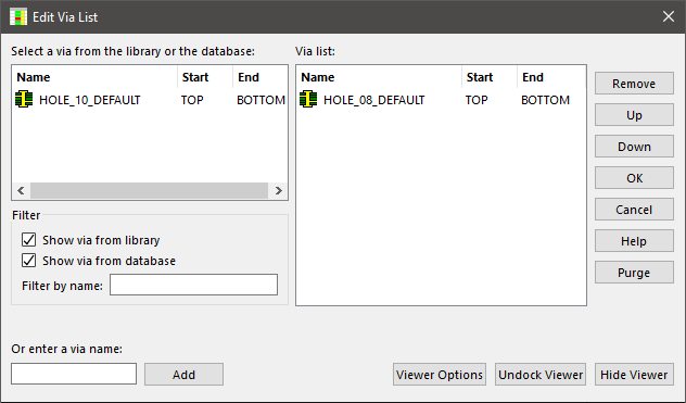
Double-click the HOLE_08_DEFAULT pad. The pad stack in now chosen as a via:
Click OK. The via has been added in the constraints manager:
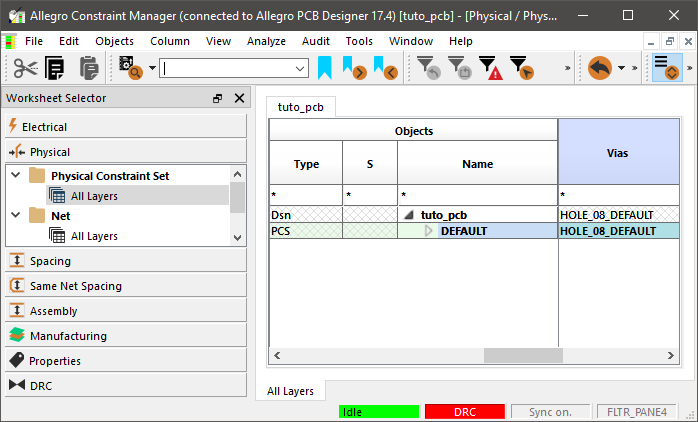
You can now close the constraints manager. You're up for double-side routing!
Start a route ![]() anywhere in the working area. The active layer is probably BOTTOM:
anywhere in the working area. The active layer is probably BOTTOM:
Then double-click at the location you want to create a via, and continue routing. If the layer has not changed to TOP, use the contextual menu to change active layer to TOP:
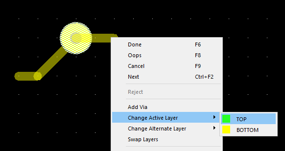
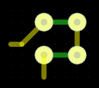
From now on, every time you double-click somewhere, a via is created and the active layer is automatically swapped:
3. More on shapes settings (ground plane)
3.1. Tuning isolation (distance from shapes to lines and pads)
Zooming in the board design, you may notice that the distance (isolation) from the ground plane to the pins (or pads) is slightly less than the one we've set in the constraint manager concerning the distance from lines to all other objects (0.2mm).
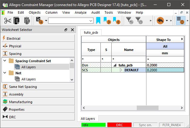
You may want to uniformize isolation distance for all kind of objects. In that case, open the constraints manager ![]() . In the Spacing category, select All Layer under Spacing Constraint Set and scroll horizontally in the spreadsheet until you find the Shape To>> column. In the Shape to All cell, enter 0.2 (mm):
. In the Spacing category, select All Layer under Spacing Constraint Set and scroll horizontally in the spreadsheet until you find the Shape To>> column. In the Shape to All cell, enter 0.2 (mm):
Repeat the above operation into the Same Net Spacing category and close the constraints manager.
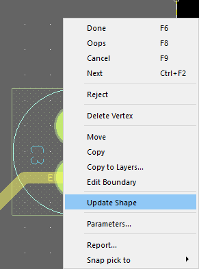
Changing isolation rules makes existing shapes to be outdated. You must perform a shape update. Use the select tool ![]() and click somewhere into the ground plane. The shape get highlighted. Then use the contextual menu Update Shape.
and click somewhere into the ground plane. The shape get highlighted. Then use the contextual menu Update Shape.
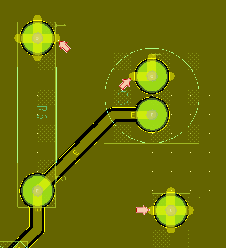
The shape is redrawn with new isolation settings:
3.2. Thermal Reliefs
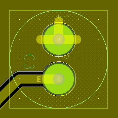
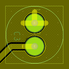
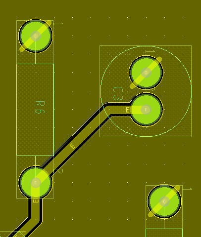
Thermal relief is the name given to the specific geometry that connects a pin to a shape on the SAME net. Common situation is component having a terminal grounded such as illustrated below:
You may wonder why a simple hole is not suitable, as one can solder directly on the plain copper plane. You would be right, but there is a thermal issue. A copper plane is a quite efficient thermal dissipator, and considering soldering iron power, it makes the soldering very difficult (the copper plane actually cools the soldering iron down). Thermal relief pattern is there to thermally isolate the soldering ring from the copper plane, while keeping electrical connection. It's a thermal resistor, and an electrical shortcut at the same time.
You can configure the geometry of the thermal relief by editing the shape properties. Make sure the editor is in idle state, and then from the main menu, select Shape→Global Dynamic Params... The Global Dynamic Shape Parameters dialog opens. In the Thermal relief connects tab, play around with some parameters (most are pretty explicit):
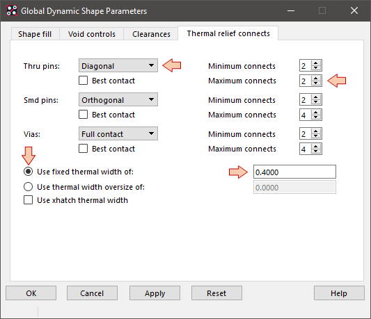
Then click Apply and watch how these parameters affect the thermal relief design:
4. Text placement
Text is very useful on PCBs to display part references, pin functions, board name... You may use the copper layer with DIY PCBs or Silkscreen layers to get text painted above the insulating varnish layer when using professional PCB manufacturing services.
To add or edit text, you may use ![]() or
or ![]() buttons. Before we do anything, let us have a look on text blocks. That's the name given by Allegro to text settings (size, spacing, width...).
buttons. Before we do anything, let us have a look on text blocks. That's the name given by Allegro to text settings (size, spacing, width...).
Use the main menu ![]() Setup→Design Parameters...
Setup→Design Parameters...
In the Design Parameter Editor dialog, select the Text tab:
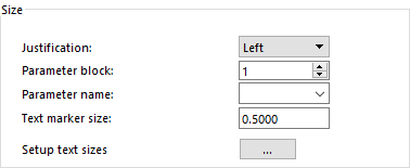
Then, click the Setup text sizes ![]() button to open the Text Setup dialog box:
button to open the Text Setup dialog box:
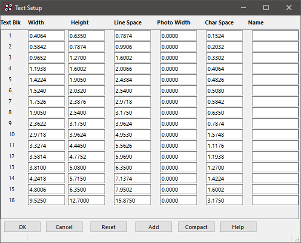
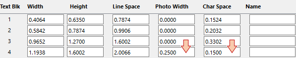
Let-us edit Text Block #4 and change:
Photo Width to 0.25 (defines line thickness)
Char Space to 0.15
Then, click OK and Apply. Close the Design Parameter Editor window.
Now click the ![]() Add Text button and review the right panel Options tabs:
Add Text button and review the right panel Options tabs:
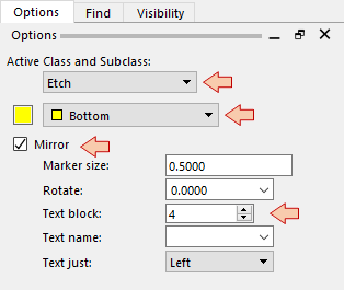
We want to name our PCB using the copper bottom layer therefore select Etch / Bottom as active class and subclass
Because we're using the bottom layer, let's check the Mirror option so that text is mirrored when seen from the top side (default editor view)
Select the text block #4 (the one we previously tuned)
Now click somewhere in the ground plane you have some room for text placement. A text-editor like cursor appears as an invitation for typing. Type what you want and then use the contextual Done:
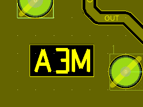
Is that "A3M"... No! If you want to see the board the way you would with the flipped real thing, just hit the Flip ![]() button:
button:
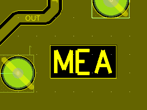
Based on this little exercise, you should now be able to add text of any size and width on any layer you like.
- Log in to post comments